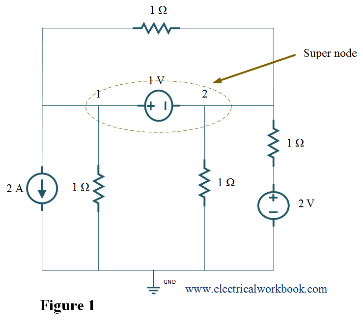
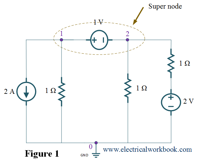
The two nonreference nodes form supernode if the voltage source (dependent or independent) is connected between two nonreference nodes. As shown below in Figure 1, 1 V voltage source is connected between nodes 1 and 2, so node 1 and node 2 forms supernode.
Procedure (steps) for applying Nodal Analysis: –
Identify the total number of nodes.
One node selected as reference node and it is assigned to have ground (zero) potential and the remaining nodes called as nonreference node and we assign voltage designations to nonreference nodes. And at last check for supernode.
Develop the KCL equations for each nonreference node.
Solve the equations to find the unknown node voltages.
Note:- Apply both KCL and KVL to determine the node voltages.
Example
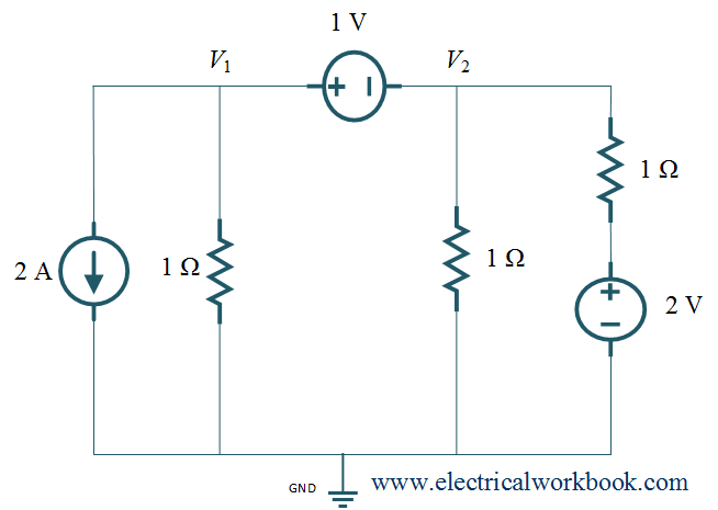
Example 1. For the given network, find nodal voltages V1 and V2.
Solution:
As shown in the above Figure, given in the question, 1 V voltage source is connected between nodes 1 and 2, so node 1 and node 2 forms supernode. Thus this problem is based on supernode.
Step 1: – The total number of nodes is 3.
Step 2: – Node 0 is selected as reference node and it is assigned to have ground (zero) potential. The remaining node 1 and node 2 are considered as non-reference node shown in Figure 1. Here, node 1 and node 2 forms supernode.
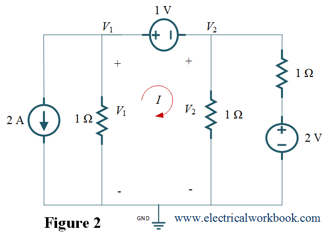
Step 3 and Step 4: – Apply both KCL and KVL to determine the node voltages.
Apply KCL to supernode as shown in Figure 2,
2+(V1–0)/1+(V2–0)/1+(V2–2)/1=0
V1+2V2=0 ……(1)
Apply KVL to the loop having current I as shown in Figure 2,
Kirchhoffs Current Law or KCL, states that the “total current or charge entering a junction or node is exactly equal to the charge leaving the node as it has no other place to go except to leave, as no charge is lost within the node“. In other words the algebraic sum of ALL the currents entering and leaving a node must be equal to zero, I(exiting) + I(entering) = 0. This idea by Kirchhoff is commonly known as the Conservation of Charge.
Kirchhoffs Current Law
Here, the three currents entering the node, I1, I2, I3 are all positive in value and the two currents leaving the node, I4 and I5 are negative in value. Then this means we can also rewrite the equation as;
I1 + I2 + I3 – I4 – I5 = 0
The term Node in an electrical circuit generally refers to a connection or junction of two or more current carrying paths or elements such as cables and components. Also for current to flow either in or out of a node a closed circuit path must exist. We can use Kirchhoff’s current law when analysing parallel circuits.
Kirchhoffs Second Law – The Voltage Law, (KVL)
Kirchhoffs Voltage Law or KVL, states that “in any closed loop network, the total voltage around the loop is equal to the sum of all the voltage drops within the same loop” which is also equal to zero. In other words the algebraic sum of all voltages within the loop must be equal to zero. This idea by Kirchhoff is known as the Conservation of Energy.
Kirchhoffs Voltage Law
Starting at any point in the loop continue in the same direction noting the direction of all the voltage drops, either positive or negative, and returning back to the same starting point. It is important to maintain the same direction either clockwise or anti-clockwise or the final voltage sum will not be equal to zero. We can use Kirchhoff’s voltage law when analysing series circuits.
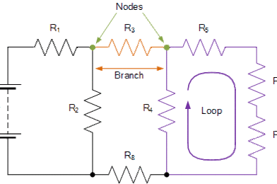
When analysing either DC circuits or AC circuits using Kirchhoffs Circuit Laws a number of definitions and terminologies are used to describe the parts of the circuit being analysed such as: node, paths, branches, loops and meshes. These terms are used frequently in circuit analysis so it is important to understand them.
Common DC Circuit Theory Terms:
• Circuit – a circuit is a closed loop conducting path in which an electrical current flows.
• Path – a single line of connecting elements or sources.
• Node – a node is a junction, connection or terminal within a circuit were two or more circuit elements are connected or joined together giving a connection point between two or more branches. A node is indicated by a dot.
• Branch – a branch is a single or group of components such as resistors or a source which are connected between two nodes.
• Loop – a loop is a simple closed path in a circuit in which no circuit element or node is encountered more than once.
• Mesh – a mesh is a single open loop that does not have a closed path. There are no components inside a mesh.
Note that:
Components are said to be connected together in Series if the same current value flows through all the components.
Components are said to be connected together in Parallel if they have the same voltage applied across them.
A Typical DC Circuit
Kirchhoffs Circuit Law Example No1
Find the current flowing in the 40Ω Resistor, R3
The circuit has 3 branches, 2 nodes (A and B) and 2 independent loops.
Using Kirchhoffs Current Law, KCL the equations are given as:
At node A : I1 + I2 = I3
At node B : I3 = I1 + I2
Using Kirchhoffs Voltage Law, KVL the equations are given as:
Loop 1 is given as : 10 = R1 I1 + R3 I3 = 10I1 + 40I3
Loop 2 is given as : 20 = R2 I2 + R3 I3 = 20I2 + 40I3
Loop 3 is given as : 10 – 20 = 10I1 – 20I2
As I3 is the sum of I1 + I2 we can rewrite the equations as;
Eq. No 1 : 10 = 10I1 + 40(I1 + I2) = 50I1 + 40I2
Eq. No 2 : 20 = 20I2 + 40(I1 + I2) = 40I1 + 60I2
We now have two “Simultaneous Equations” that can be reduced to give us the values of I1 and I2
Substitution of I1 in terms of I2 gives us the value of I1 as -0.143 Amps
Substitution of I2 in terms of I1 gives us the value of I2 as +0.429 Amps
As : I3 = I1 + I2
The current flowing in resistor R3 is given as : -0.143 + 0.429 = 0.286 Amps
and the voltage across the resistor R3 is given as : 0.286 x 40 = 11.44 volts
The negative sign for I1 means that the direction of current flow initially chosen was wrong, but never the less still valid. In fact, the 20v battery is charging the 10v battery.
Application of Kirchhoffs Circuit Laws
These two laws enable the Currents and Voltages in a circuit to be found, ie, the circuit is said to be “Analysed”, and the basic procedure for using Kirchhoff’s Circuit Laws is as follows:
1. Assume all voltages and resistances are given. ( If not label them V1, V2,… R1, R2, etc. )
2. Label each branch with a branch current. ( I1, I2, I3 etc. )
3. Find Kirchhoff’s first law equations for each node.
4. Find Kirchhoff’s second law equations for each of the independent loops of the circuit.
5. Use Linear simultaneous equations as required to find the unknown currents.
As well as using Kirchhoffs Circuit Law to calculate the various voltages and currents circulating around a linear circuit, we can also use loop analysis to calculate the currents in each independent loop which helps to reduce the amount of mathematics required by using just Kirchhoff’s laws. In the next tutorial about DC circuits, we will look at Mesh Current Analysis to do just that.
Amplifiers or any operational amplifier for that matter and these are.
No Current Flows into the Input Terminals
The Differential Input Voltage is Zero as V1 = V2 = 0 (Virtual Earth)
Then by using these two rules we can derive the equation for calculating the closed-loop gain of an inverting amplifier, using first principles.
Current ( i ) flows through the resistor network as shown.
Then, the Closed-Loop Voltage Gain of an Inverting Amplifier is given as.
and this can be transposed to give Vout as:
Non-inverting
In the previous Inverting Amplifier tutorial, we said that for an ideal op-amp “No current flows into the input terminal” of the amplifier and that “V1 always equals V2”. This was because the junction of the input and feedback signal ( V1 ) are at the same potential.
In other words the junction is a “virtual earth” summing point. Because of this virtual earth node the resistors, Rƒ and R2 form a simple potential divider network across the non-inverting amplifier with the voltage gain of the circuit being determined by the ratios of R2 and Rƒ as shown below.
Equivalent Potential Divider Network
Then using the formula to calculate the output voltage of a potential divider network, we can calculate the closed-loop voltage gain ( AV ) of the Non-inverting Amplifier as follows:
Then the closed loop voltage gain of a Non-inverting Operational Amplifier will be given as:
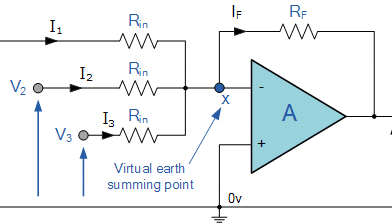
Summing
In this simple summing amplifier circuit, the output voltage, ( Vout ) now becomes proportional to the sum of the input voltages, V1, V2, V3, etc. Then we can modify the original equation for the inverting amplifier to take account of these new inputs thus:
However, if all the input impedances, ( RIN ) are equal in value, we can simplify the above equation to give an output voltage of:
Summing Amplifier Equation
Differential Amplifier
By connecting each input in turn to 0v ground we can use superposition to solve for the output voltage Vout. Then the transfer function for a Differential Amplifier circuit is given as:
When resistors, R1 = R2 and R3 = R4 the above transfer function for the differential amplifier can be simplified to the following expression:
Differential Amplifier Equation
Op-amp Integrator Circuit
To simplify the math’s a little, this can also be re-written as:
notes: if Vin is constant voltage so Rin voltage drop always equal Vin so it is feeding C with constant current source for example if we have capacitor with 1H and constant current source 1A every seconds the capacitor it will increase 1 volt constantly Vin/(Rin.C)
Operational amplifiers are linear devices that have all the properties required for nearly ideal DC amplification and are therefore used extensively in signal conditioning, filtering or to perform mathematical operations such as add, subtract, integration and differentiation.
An Operational Amplifier, or op-amp for short, is fundamentally a voltage amplifying device designed to be used with external feedback components such as resistors and capacitors between its output and input terminals. These feedback components determine the resulting function or “operation” of the amplifier and by virtue of the different feedback configurations whether resistive, capacitive or both, the amplifier can perform a variety of different operations, giving rise to its name of “Operational Amplifier”.
An Operational Amplifier is basically a three-terminal device which consists of two high impedance inputs. One of the inputs is called the Inverting Input, marked with a negative or “minus” sign, ( – ). The other input is called the Non-inverting Input, marked with a positive or “plus” sign ( + ).
A third terminal represents the operational amplifiers output port which can both sink and source either a voltage or a current. In a linear operational amplifier, the output signal is the amplification factor, known as the amplifiers gain ( A ) multiplied by the value of the input signal and depending on the nature of these input and output signals, there can be four different classifications of operational amplifier gain.
Voltage – Voltage “in” and Voltage “out”
Current – Current “in” and Current “out”
Transconductance – Voltage “in” and Current “out”
Transresistance – Current “in” and Voltage “out”
Since most of the circuits dealing with operational amplifiers are voltage amplifiers, we will limit the tutorials in this section to voltage amplifiers only, (Vin and Vout).
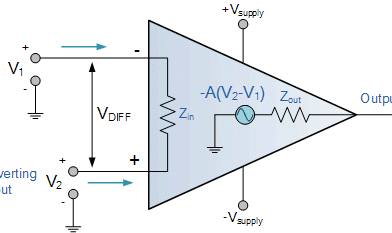
The output voltage signal from an Operational Amplifier is the difference between the signals being applied to its two individual inputs. In other words, an op-amps output signal is the difference between the two input signals as the input stage of an Operational Amplifier is in fact a differential amplifier as shown below.
Differential Amplifier
The circuit below shows a generalized form of a differential amplifier with two inputs marked V1 and V2. The two identical transistors TR1 and TR2 are both biased at the same operating point with their emitters connected together and returned to the common rail, -Vee by way of resistor Re.
Differential Amplifier
The circuit operates from a dual supply +Vcc and -Vee which ensures a constant supply. The voltage that appears at the output, Vout of the amplifier is the difference between the two input signals as the two base inputs are in anti-phase with each other.
So as the forward bias of transistor, TR1 is increased, the forward bias of transistor TR2 is reduced and vice versa. Then if the two transistors are perfectly matched, the current flowing through the common emitter resistor, Re will remain constant.
Like the input signal, the output signal is also balanced and since the collector voltages either swing in opposite directions (anti-phase) or in the same direction (in-phase) the output voltage signal, taken from between the two collectors is, assuming a perfectly balanced circuit the zero difference between the two collector voltages.
This is known as the Common Mode of Operation with the common mode gain of the amplifier being the output gain when the input is zero.
Operational Amplifiers also have one output (although there are ones with an additional differential output) of low impedance that is referenced to a common ground terminal and it should ignore any common mode signals that is, if an identical signal is applied to both the inverting and non-inverting inputs there should no change to the output.
However, in real amplifiers there is always some variation and the ratio of the change to the output voltage with regards to the change in the common mode input voltage is called the Common Mode Rejection Ratio or CMRR for short.
Operational Amplifiers on their own have a very high open loop DC gain and by applying some form of Negative Feedback we can produce an operational amplifier circuit that has a very precise gain characteristic that is dependant only on the feedback used. Note that the term “open loop” means that there are no feedback components used around the amplifier so the feedback path or loop is open.
An operational amplifier only responds to the difference between the voltages on its two input terminals, known commonly as the “Differential Input Voltage” and not to their common potential. Then if the same voltage potential is applied to both terminals the resultant output will be zero. An Operational Amplifiers gain is commonly known as the Open Loop Differential Gain, and is given the symbol (Ao).
Equivalent Circuit of an Ideal Operational Amplifier
Op-amp Parameter and Idealised Characteristic
Open Loop Gain, (Avo)
Infinite – The main function of an operational amplifier is to amplify the input signal and the more open loop gain it has the better. Open-loop gain is the gain of the op-amp without positive or negative feedback and for such an amplifier the gain will be infinite but typical real values range from about 20,000 to 200,000.
Input impedance, (ZIN)
Infinite – Input impedance is the ratio of input voltage to input current and is assumed to be infinite to prevent any current flowing from the source supply into the amplifiers input circuitry ( IIN = 0 ). Real op-amps have input leakage currents from a few pico-amps to a few milli-amps.
Output impedance, (ZOUT)
Zero – The output impedance of the ideal operational amplifier is assumed to be zero acting as a perfect internal voltage source with no internal resistance so that it can supply as much current as necessary to the load. This internal resistance is effectively in series with the load thereby reducing the output voltage available to the load. Real op-amps have output impedances in the 100-20kΩ range.
Bandwidth, (BW)
Infinite – An ideal operational amplifier has an infinite frequency response and can amplify any frequency signal from DC to the highest AC frequencies so it is therefore assumed to have an infinite bandwidth. With real op-amps, the bandwidth is limited by the Gain-Bandwidth product (GB), which is equal to the frequency where the amplifiers gain becomes unity.
Offset Voltage, (VIO)
Zero – The amplifiers output will be zero when the voltage difference between the inverting and the non-inverting inputs is zero, the same or when both inputs are grounded. Real op-amps have some amount of output offset voltage.
From these “idealized” characteristics above, we can see that the input resistance is infinite, so no current flows into either input terminal (the “current rule”) and that the differential input offset voltage is zero (the “voltage rule”). It is important to remember these two properties as they will help us understand the workings of the Operational Amplifier with regards to the analysis and design of op-amp circuits.
However, real Operational Amplifiers such as the commonly available uA741, for example do not have infinite gain or bandwidth but have a typical “Open Loop Gain” which is defined as the amplifiers output amplification without any external feedback signals connected to it and for a typical operational amplifier is about 100dB at DC (zero Hz). This output gain decreases linearly with frequency down to “Unity Gain” or 1, at about 1MHz and this is shown in the following open loop gain response curve.
Open-loop Frequency Response Curve
From this frequency response curve we can see that the product of the gain against frequency is constant at any point along the curve. Also that the unity gain (0dB) frequency also determines the gain of the amplifier at any point along the curve. This constant is generally known as the Gain Bandwidth Product or GBP. Therefore:
GBP = Gain x Bandwidth = A x BW
For example, from the graph above the gain of the amplifier at 100kHz is given as 20dB or 10, then the gain bandwidth product is calculated as:
GBP = A x BW = 10 x 100,000Hz = 1,000,000.
Similarly, the operational amplifiers gain at 1kHz = 60dB or 1000, therefore the GBP is given as:
GBP = A x BW = 1,000 x 1,000Hz = 1,000,000. The same!.
The Voltage Gain (AV) of the operational amplifier can be found using the following formula:
and in Decibels or (dB) is given as:
An Operational Amplifiers Bandwidth
The operational amplifiers bandwidth is the frequency range over which the voltage gain of the amplifier is above 70.7% or -3dB (where 0dB is the maximum) of its maximum output value as shown below.
Here we have used the 40dB line as an example. The -3dB or 70.7% of Vmax down point from the frequency response curve is given as 37dB. Taking a line across until it intersects with the main GBP curve gives us a frequency point just above the 10kHz line at about 12 to 15kHz. We can now calculate this more accurately as we already know the GBP of the amplifier, in this particular case 1MHz.
Operational Amplifier Example No1.
Using the formula 20 log (A), we can calculate the bandwidth of the amplifier as:
GBP ÷ A = Bandwidth, therefore, 1,000,000 ÷ 70.8 = 14,124Hz, or 14kHz
Then the bandwidth of the amplifier at a gain of 40dB is given as 14kHz as previously predicted from the graph.
Operational Amplifier Example No2.
If the gain of the operational amplifier was reduced by half to say 20dB in the above frequency response curve, the -3dB point would now be at 17dB. This would then give the operational amplifier an overall gain of 7.08, therefore A = 7.08.
If we use the same formula as above, this new gain would give us a bandwidth of approximately 141.2kHz, ten times more than the frequency given at the 40dB point. It can therefore be seen that by reducing the overall “open loop gain” of an operational amplifier its bandwidth is increased and visa versa.
In other words, an operational amplifiers bandwidth is inversely proportional to its gain, ( A 1/∞ BW ). Also, this -3dB corner frequency point is generally known as the “half power point”, as the output power of the amplifier is at half its maximum value as shown:
Regenerative switching circuits such as Astable Multivibrators are the most commonly used type of relaxation oscillator because not only are they simple, reliable and ease of construction they also produce a constant square wave output waveform.
Unlike the Monostable Multivibrator or the Bistable Multivibrator we looked at in the previous tutorials that require an “external” trigger pulse for their operation, the Astable Multivibrator has automatic built in triggering which switches it continuously between its two unstable states both set and reset.
The Astable Multivibrator is another type of cross-coupled transistor switching circuit that has NO stable output states as it changes from one state to the other all the time. The astable circuit consists of two switching transistors, a cross-coupled feedback network, and two time delay capacitors which allows oscillation between the two states with no external triggering to produce the change in state.
In electronic circuits, astable multivibrators are also known as Free-running Multivibrator as they do not require any additional inputs or external assistance to oscillate. Astable oscillators produce a continuous square wave from its output or outputs, (two outputs no inputs) which can then be used to flash lights or produce a sound in a loudspeaker.
The basic transistor circuit for an Astable Multivibrator produces a square wave output from a pair of grounded emitter cross-coupled transistors. Both transistors either NPN or PNP, in the multivibrator are biased for linear operation and are operated as Common Emitter Amplifiers with 100% positive feedback.
This configuration satisfies the condition for oscillation when: ( βA = 1∠ 0o ). This results in one stage conducting “fully-ON” (Saturation) while the other is switched “fully-OFF” (cut-off) giving a very high level of mutual amplification between the two transistors. Conduction is transferred from one stage to the other by the discharging action of a capacitor through a resistor as shown below.
Basic Astable Multivibrator Circuit
Assume a 6 volt supply and that transistor, TR1 has just switched “OFF” (cut-off) and its collector voltage is rising towards Vcc, meanwhile transistor TR2 has just turned “ON”. Plate “A” of capacitor C1 is also rising towards the +6 volts supply rail of Vcc as it is connected to the collector of TR1 which is now cut-off. Since TR1 is in cut-off, it conducts no current so there is no volt drop across load resistor R1.
The other side of capacitor, C1, plate “B”, is connected to the base terminal of transistor TR2 and at 0.6v because transistor TR2 is conducting (saturation). Therefore, capacitor C1 has a potential difference of +5.4 volts across its plates, (6.0 – 0.6v) from point A to point B.
Since TR2 is fully-on, capacitor C2 starts to charge up through resistor R2 towards Vcc. When the voltage across capacitor C2 rises to more than 0.6v, it biases transistor TR1 into conduction and into saturation.
The instant that transistor, TR1 switches “ON”, plate “A” of the capacitor which was originally at Vcc potential, immediately falls to 0.6 volts. This rapid fall of voltage on plate “A” causes an equal and instantaneous fall in voltage on plate “B” therefore plate “B” of C1 is pulled down to -5.4v (a reverse charge) and this negative voltage swing is applied the base of TR2 turning it hard “OFF”. One unstable state.
Transistor TR2 is driven into cut-off so capacitor C1 now begins to charge in the opposite direction via resistor R3 which is also connected to the +6 volts supply rail, Vcc. Thus the base of transistor TR2 is now moving upwards in a positive direction towards Vcc with a time constant equal to the C1 x R3 combination.
However, it never reaches the value of Vcc because as soon as it gets to 0.6 volts positive, transistor TR2 turns fully “ON” into saturation. This action starts the whole process over again but now with capacitor C2 taking the base of transistor TR1 to -5.4v while charging up via resistor R2 and entering the second unstable state.
Then we can see that the circuit alternates between one unstable state in which transistor TR1 is “OFF” and transistor TR2 is “ON”, and a second unstable in which TR1 is “ON” and TR2 is “OFF” at a rate determined by the RC values. This process will repeat itself over and over again as long as the supply voltage is present.
The amplitude of the output waveform is approximately the same as the supply voltage, Vcc with the time period of each switching state determined by the time constant of the RC networks connected across the base terminals of the transistors. As the transistors are switching both “ON” and “OFF”, the output at either collector will be a square wave with slightly rounded corners because of the current which charges the capacitors. This could be corrected by using more components as we will discuss later.
If the two time constants produced by C2 x R2 and C1 x R3 in the base circuits are the same, the mark-to-space ratio ( t1/t2 ) will be equal to one-to-one making the output waveform symmetrical in shape. By varying the capacitors, C1, C2 or the resistors, R2, R3 the mark-to-space ratio and therefore the frequency can be altered.
We saw in the RC Discharging tutorial that the time taken for the voltage across a capacitor to fall to half the supply voltage, 0.5Vcc is equal to 0.69 time constants of the capacitor and resistor combination. Then taking one side of the astable multivibrator, the length of time that transistor TR2 is “OFF” will be equal to 0.69T or 0.69 times the time constant of C1 x R3. Likewise, the length of time that transistor TR1 is “OFF” will be equal to 0.69T or 0.69 times the time constant of C2 x R2 and this is defined as.
Astable Multivibrators Periodic Time
Where, R is in Ω’s and C in Farads.
By altering the time constant of just one RC network the mark-to-space ratio and frequency of the output waveform can be changed but normally by changing both RC time constants together at the same time, the output frequency will be altered keeping the mark-to-space ratios the same at one-to-one.
If the value of the capacitor C1 equals the value of the capacitor, C2, C1 = C2 and also the value of the base resistor R2 equals the value of the base resistor, R3, R2 = R3 then the total length of time of the Multivibrators cycle is given below for a symmetrical output waveform.
Frequency of Oscillation
Where, R is in Ω’s, C is in Farads, T is in seconds and ƒ is in Hertz.
and this is known as the “Pulse Repetition Frequency”. So Astable Multivibrators can produce TWO very short square wave output waveforms from each transistor or a much longer rectangular shaped output either symmetrical or non-symmetrical depending upon the time constant of the RC network as shown below.
Astable Multivibrator Waveforms
Astable Multivibrator Example No1
An Astable Multivibrators circuit is required to produce a series of pulses at a frequency of 500Hz with a mark-to-space ratio of 1:5. If R2 = R3 = 100kΩ, calculate the values of the capacitors, C1 and C2 required.
and by rearranging the formula above for the periodic time, the values of the capacitors required to give a mark-to-space ratio of 1:5 are given as:
The values of 4.83nF and 24.1nF respectively, are calculated values, so we would need to choose the nearest preferred values for C1 and C2 allowing for the capacitors tolerance. In fact due to the wide range of tolerances associated with the humble capacitor the actual output frequency may differ by as much as ±20%, (400 to 600Hz in our simple example) from the actual frequency needed.
If we require the output astable waveform to be non-symmetrical for use in timing or gating type circuits, etc, we could manually calculate the values of R and C for the individual components required as we did in the example above. However, when the two R’s and C´s are both equal, we can make our life a little bit easier for ourselves by using tables to show the astable multivibrators calculated frequencies for different combinations or values of both R and C. For example,
Astable Multivibrator Frequency Table
Res.
Capacitor Values
1nF
2.2nF
4.7nF
10nF
22nF
47nF
100nF
220nF
470nF
1.0kΩ
714.3kHz
324.6kHz
151.9kHz
71.4kHz
32.5kHz
15.2kHz
7.1kHz
3.2kHz
1.5kHz
2.2kΩ
324.7kHz
147.6kHz
69.1kHz
32.5kHz
14.7kHz
6.9kHz
3.2kHz
1.5kHz
691Hz
4.7kΩ
151.9kHz
69.1kHz
32.3kHz
15.2kHz
6.9kHz
3.2kHz
1.5kHz
691Hz
323Hz
10kΩ
71.4kHz
32.5kHz
15.2kHz
7.1kHz
3.2kHz
1.5kHz
714Hz
325Hz
152Hz
22kΩ
32.5kHz
14.7kHz
6.9kHz
3.2kHz
1.5kHz
691Hz
325Hz
147Hz
69.1Hz
47kΩ
15.2kHz
6.9kHz
3.2kHz
1.5kHz
691Hz
323Hz
152Hz
69.1Hz
32.5Hz
100kΩ
7.1kHz
3.2kHz
1.5kHz
714Hz
325Hz
152Hz
71.4Hz
32.5Hz
15.2Hz
220kΩ
3.2kHz
1.5kHz
691Hz
325Hz
147Hz
69.1Hz
32.5Hz
15.2Hz
6.9Hz
470kΩ
1.5kHz
691Hz
323Hz
152Hz
69.1Hz
32.5Hz
15.2Hz
6.6Hz
3.2Hz
1MΩ
714Hz
325Hz
152Hz
71.4Hz
32.5Hz
15.2Hz
6.9Hz
3.2Hz
1.5Hz
Pre-calculated frequency tables can be very useful in determining the required values of both R and C for a particular symmetrical output frequency without the need to keep recalculating them every time a different frequency is required.
By changing the two fixed resistors, R2 and R3 for a dual-ganged potentiometer and keeping the values of the capacitors the same, the frequency from the Astable Multivibrators output can be more easily “tuned” to give a particular frequency value or to compensate for the tolerances of the components used.
For example, selecting a capacitor value of 10nF from the table above. By using a 100kΩ’s potentiometer for our resistance, we would get an output frequency that can be fully adjusted from slightly above 71.4kHz down to 714Hz, some 3 decades of frequency range. Likewise a capacitor value of 47nF would give a frequency range from 152Hz to well over 15kHz.
Astable Multivibrator Example No2
An Astable Multivibrator circuit is constructed using two timing capacitors of equal value of 3.3uF and two base resistors of value 10kΩ. Calculate the minimum and maximum frequencies of oscillation if a 100kΩ dual-gang potentiometer is connected in series with the two resistors.
With the potentiometer at 0%, the value of the base resistance is equal to 10kΩ.
with the potentiometer at 100%, the value of the base resistance is equal to 10kΩ + 100kΩ = 110kΩ.
Then the output frequency of oscillation for the astable multivibrator can be varied from between 2.0 and 22 Hertz.
When selecting both the resistance and capacitance values for reliable operation, the base resistors should have a value that allows the transistor to turn fully “ON” when the other transistor turns “OFF”. For example, consider the circuit above. When transistor TR2 is fully “ON”, (saturation) nearly the same voltage is dropped across resistor R3 and resistor R4.
If the transistor being used has a current gain, β of 100 and the collector load resistor, R4 is equal to say 1kΩ the maximum base resistor value would therefore be 100kΩ. Any higher and the transistor may not turn fully “ON” resulting in the multivibrator giving erratic results or not oscillate at all. Likewise, if the value of the base resistor is too low the transistor may not switch “OFF” and the multivibrator would again not oscillate.
An output signal can be obtained from the collector terminal of either transistor in the Astable Multivibrators circuit with each output waveform being a mirror image of itself. We saw above that the leading edge of the output waveform is slightly rounded and not square due to the charging characteristics of the capacitor in the cross-coupled circuit.
But we can introduce another transistor into the circuit that will produce an almost perfectly square output pulse and which can also be used to switch higher current loads or low impedance loads such as LED’s or loudspeakers, etc without affecting the operation of the actual astable multivibrator. However, the down side to this is that the output waveform is not perfectly symmetrical as the additional transistor produces a very small delay. Consider the two circuits below.
Astable Multivibrators Driving Circuit
An output with a square leading edge is now produced from the third transistor, TR3 connected to the emitter of transistor, TR2. This third transistor switches “ON” and “OFF” in unison with transistor TR2. We can use this additional transistor to switch Light Emitting Diodes, Relays or to produce a sound from a Sound Transducer such as a speaker or piezo sounder as shown above.
The load resistor, Rx needs to be suitably chosen to take into account the forward volt drops and to limit the maximum current to about 20mA for the LED circuit or to give a total load impedance of about 100Ω for the speaker circuit. The speaker can have any impedance less than 100Ω.
By connecting an additional transistor, TR4 to the emitter circuit of the other transistor, TR1 in a similar fashion we can produce an astable multivibrator circuit that will flash two sets of lights or LED’s from one to the other at a rate determined by the time constant of the RC timing network.
In the next tutorial about Waveforms and Signals, we will look at the different types of Astable Multivibrators that are used to produce a continuous output waveform. These circuits known as relaxation oscillators produce either a square or rectangular wave at their outputs for use in sequential circuits as either a clock pulse or timing signal. These types of circuits are called Waveform Generators.