Inductive spiking And Flyback Diode

Flyback Voltage and its Origin

A Flyback voltage or an Inductive Flyback is a voltage spike created by an inductor when its power supply is removed abruptly. The reason for this voltage spike is the fact that there cannot be an instant change to the current flowing through an Inductor.

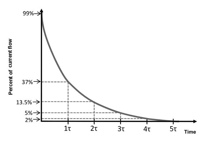
Time Constant of the Inductor determines the rate at which the current can change through an inductor. This is similar to the time constant of a Capacitor, which determines the rate at which its voltage can change.

Time Constant of Inductor τ = L/R, where L is Inductance in Henries and R is series resistance in Ohms.

Similar to a capacitor, it takes nearly 5 time constants (5τ) to dissipate the current in an inductor.

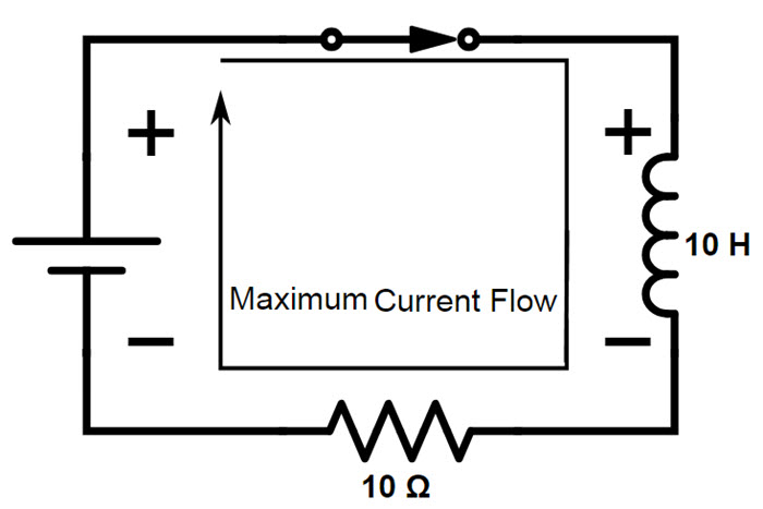
Assume, in the above circuit, the inductor is 10H and the series resistor is 10Ω. So, when the switch is closed, maximum current flows through the inductor.

Flyback Diode Current Flow through Inductor

Now, let us see what happens when the switch is opened suddenly.

Flyback Diode No Current Flow through Inductor

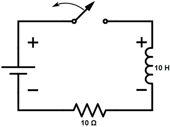
First, let us calculate the time constant. Using the formula of time constant and substituting the above assumed values, it is clear that the time constant is 1 second.

So, it will take approximately 5 seconds from the moment the switch is open, to completely stop the flow of current. This means that current flows in the circuit even after the switch is open (assuming it would take a few milli seconds to completely open the switch). How is this possible?

This can be understood from the inductors point of view. The switch gap, which is essentially air, is viewed as a huge resistor by the inductor and the resistance is in the order of few mega Ohms. This means that the circuit is still closed from inductor’s point of view with a huge resistor filling in the air gap.

Now that it is confirmed that the circuit is still closed, the inductor will try to dissipate the current and in order to do so, the inductor will drop voltage across the air gap resistance by reversing its polarity by using the energy stored in it in the form of magnetic field.

Flyback Diode Flyback Voltage Origin

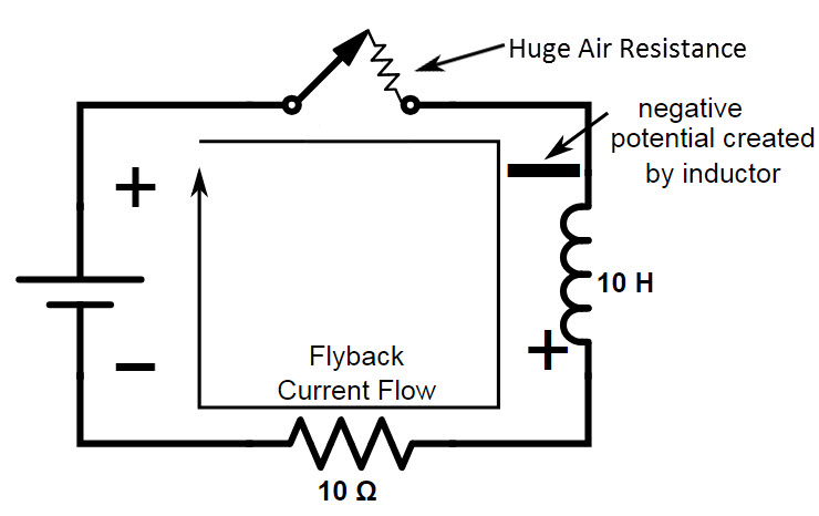
Now, the inductor tries to flow current as per its current dissipation curve. This could be problematic according to Ohm’s Law, V = I x R.

Even for a small current, when it is multiplied by the huge air resistance (few hundreds of Mega Ohms) will lead to a very high voltage across the air resistor. This is the origin of the Flyback Voltage or Voltage Spike.

Impact of Flyback Voltage on Switches

As there is no physical resistor when the switch is opened, sparks / arcs will occur between the switch and the other terminal, if a mechanical switch is used. All the energy from the arc is usually discharged across the contacts of the switch in the form of heat.

This could potentially damage the switches permanently or drastically reduce the lifetime of the switches. when speaking of switches, they can be mechanical switches or semiconductor switches like Transistors.

How Flyback Diode can prevent Voltage Spikes?

To protect the switch from being damaged due voltage spikes or inductive Flyback, a Flyback Diode or a Freewheeling Diode is used. The basic idea behind the use of a Flyback Diode is to provide an alternative path for the inductor for its current to flow.

Flyback Diode using Flyback Diode

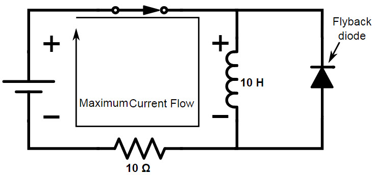
The above image shows the same inductor circuit but with additionally a Flyback Diode. It is important to note that the diode is connected in reverse bias when the switch is closed.

As a result, the diode doesn’t impact the operation of the rest of the circuit when the switch is closed and maximum current flows through the inductor.

Flyback Diode Open Circuit with Flyback Diode

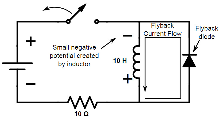
But when the switch is opened, the change in polarity of the inductor will make the diode to be placed in forward bias. Hence, the diode will allow current to flow at a rate determined by the time constant of the inductor.

The resistance of the diode, when it is forward biased, is very less and hence the voltage drop across the diode will be significantly less for the current to flow. This prevents arc at the switching device and as a result protects the switching device from damage.

Reverse Polarity Protection

eries Diode – By far the cheapest and easiest to install is a diode in series with the positive power lead. Anode toward the power supply and Cathode (banded end) going to the radio. For a few pennies a 1N400x series diode will handle many QRP rigs up to 1A and a 1N540x series will work up to 3A. Although simple and cheap it comes at a cost. The diode will drop about 0.6-0.9V which could result in lower transmit power and if the equipment uses voltage regulators this lower voltage may be under the regulator level.

RPP-Diode

Bridge Rectifier – The most foolproof for reverse polarity protection. For about a dollar or two, the bridge will correct the polarity no matter how you connect the power supply. With a bridge there are always 2 diodes conducting which can result in greater losses of round .8-1.5V.   This works good only when a single power supply is used with a single radio but should be avoided when multiple pieces of equipment are connected together via the grounds.

RPP-Bridge-Fixed

Fuse with crowbar diode – With most protection circuits there is usually some form of loss in the process, as seen in the diode examples above. However, the fuse with crowbar diode has no voltage drop loss. The crowbar works by putting a diode across the voltage lines with the Cathode toward the positive side. This in effect leaves the path through the diode open unless the polarity is reversed. When that happens the diode now becomes an almost short circuit causing the fuse to blow. The cost of course if that a hefty diode needs to be used to handle the large current flow until the fuse opens up, not to mention a new fuse each time it’s tested.

RPP-Crowbar

MOSFET1 – Not only can MOFSET’s do a great job at switching, a P-channel MOSFET does an excellent job of reverse polarity protection. Depending on your needs the cost is from a few pennies to a dollar or two. Under normal circumstances the MOSFET is turned on with a small voltage drop across it, typically fractions less than the diode example above. When the polarity is reversed the MOSFET is forced off and creates an open circuit. See the sidebar on MOSFET selection for more information in selecting a P-channel MOSFET.

RPP-MOSFET

MOSFET RPP Rules:

  1. VDS – Voltage Drain to Source – must be greater than the power supply voltage.
  2. RDS(on) – Resistance of the Drain to Source when the MOSFET is turned on. This must be as low as possible. Usually the lower the Rds(on) the more expensive.
  3. Vgss – Voltage from Gate to Source – The maximum voltage allowed from Gate to Source. This should also be greater than the power supply voltage. Many MOSFET’s will have a lower Vgss. In these cases the addition of a simple zener diode and resistor are required as follows:
    1. Resistor is not critical, almost any value between 10K and 100K is good.
    2. Zener voltage must be less than the MOSFET Vgss. Additionally it must be greater than the MOSFET Vgs(th) – Threshold Voltage from Gate to Source – This is the minimum voltage required to fully turn on the MOSFET.
  4. There is a small capacitor in the Drain to Gate circuitry. This capacitor is optional but recommended and only used for static discharge protection.2
RPP-MOSFET-low

Transistor Capacitance Multiplier

The basic capacitance multiplier circuit is essentially a simple emitter follower with a capacitor on the base and a feed resistor from the input to the base to turn the transistor on. A capacitor from the base to ground provides the smoothing.

Basic transistor capacitance multiplier circuit
Basic transistor capacitance multiplier

The capacitance multiplier circuit operation is quite straightforward. It acts as a simple emitter follower. The resistor R1 provides bias for the base emitter junction, and the capacitor provides smoothing. This considerably reduces the levels on noise on the output, i.e. Vout.

The effect of placing the transistor in the circuit is that it effectively multiplies the capacitance on the base by the current gain of the transistor, i.e. by β

The capacitance multiplier circuit is not a voltage regulator. The output voltage varies directly with the input Vin as there is no voltage reference. Generally the output voltage is about 0.65V less than the base voltage, and around 2 – 3 V less than Vin when a load is applied.

The ripple and noise levels on the output can be reduced to very low levels> Increasing the values of R1 and C1 reduce the output ripple, and increasingly at low frequencies. On the downside large values of R1 and C1 cause the output to rise slowly towards the required value after turn on, because of the large time constant of R1 and C1.

Modified capacitance multiplier

The drawback of the circuit is that in its basic form, there is very little voltage drop across the series pass transistor, and noise reduction is not as high as it may be. To overcome this, some people place a resistor across the capacitor and this provides a potential divider reducing the voltage at the base and increasing the voltage drop across the transistor. This enables it to provide better noise reduction, although it does increase power dissipation and reduces the voltage at Vout.

Basic transistor capacitance multiplier circuit incorporating a bias potential divider
Basic transistor capacitance multiplier with a potential divider

This version of the capacitance multiplier circuit includes an additional resistor from the base to ground to reduce the base voltage and provide additional voltage drop across the transistor for improved smoothing. This is more important when the levels of ripple are higher.

Typically the voltage through the potential divider should be sufficient to maintain the base voltage sufficiently. A judgement can be made regarding the level of current though the potential divider, but often in these types of circuits it may be ten times the base current. This would ensure that the emitter voltage is maintained over a wide range of output current levels.

Example application for a capacitance multiplier

The power supply shown here provides only smoothing at this stage and no stabilisation or voltage regulation. The input is taken from the mains and rectified by the bridge rectifier. It then passes into a smoothing capacitor, C1, to provide the first smoothing and remove the major ripple. This capacitor should have a large ripple current capability if the supply is to be used for high current levels.

It should be remembered that the capacitance multiplication effect can only be realised if there is a sufficient voltage drop across the series transistor. Typically this should be a minimum of 3 volts at all times.

The capacitor C2 is connected to the base of the transistor TR1. This provides the capacitance for the capacitance multiplication effect.

TR1 is the main pass transistor and must be able to drop the required voltage and at the required current, so power dissipation may need to be calculated.

Example application for a capacitance multiplier

On the output there is a capacitor to provide a little further decoupling and to ensure that the circuit remains stable. The resistor ensures the output voltage drains away at power removal. The diode D1 ensures that the transistor does not become reverse biased.

Unusual Transistors Circuits

Diod Transistors

Transistor as a Zener

Zener diodes connected as shown in Fig. 1 are carefully doped at manufacture such that they break down when a critical reverse bias voltage is applied and allows current to flow. The current is limited by the power ratings of the particular device employed.

Zeners are used to provide a voltage reference and any transistor can be employed to do the same job if connected as shown in Fig. 2.

Different transistors will produce different zener voltages and a series of tests can be done to establish what the typical zener voltage is for that device.

A suitable setup could be employed as shown below.

  A BC548B gives a zener voltage Vz = 8.2V

  A BC549B gives a zener voltage Vz = 10.8V

  A BC547B gives a zener voltage Vz = 9.1V

  A BC184 gives a zener voltage Vz = 8.2V

Using the Configuration in Practice

The above circuit Fig 4 could form the basis of a low power regulated power supply.

Vbe Multiplayer

Variable Reference Voltage Circuit

Fig. 5 shows a way of adjusting the voltage Vz to suit by adjusting the resistor values of R1 and R2.

Vz = Vbe((R1 + R2)/R2)

Better regulation can be achieved with a darlington configuration as shown below where it is used in a simple regulated supply, but now the voltage Vz becomes:-

Vz = 2Vbe((R1 + R2)/R2)

and the regulated output voltage becomes:-

Vo = Vz – Vbe

Other more circuits

any signal add to it vbe by Q1 and send it to Q2 so Q2 can read any signal
vce more stable than vbe because once vbe increased R2 incresed and keep palance
Vbe multiplayer with more stability