Fan-out is a term that defines the maximum number of digital inputs that the output of a single logic gate can feed. Most transistor-transistor logic ( TTL ) gates can feed up to 10 other digital gates or devices. Thus, a typical TTL gate has a fan-out of 10.
In some digital systems, it is necessary for a single TTL logic gate to drive more than 10 other gates or devices. When this is the case, a device called a buffer can be used between the TTL gate and the multiple devices it must drive. A buffer of this type has a fan-out of 25 to 30. A logical inverter (also called a NOT gate) can serve this function in most digital circuits.
Buffer
Two inverter, or NOT, gates connected in “series” so as to invert, then re-invert, a binary bit perform the function of a buffer. Buffer gates merely serve the purpose of signal amplification: taking a “weak” signal source that isn’t capable of sourcing or sinking much current, and boosting the current capacity of the signal so as to be able to drive a load.
Buffer circuits are symbolized by a triangle symbol with no inverter “bubble.”
Buffers, like inverters, may be made in open-collector output or totem pole output forms
Open Collector OR Open Drain
Tri-state
Three-state logic is a logic used in electronic circuits wherein a third state, the high-impedance state
Three-state logic is used to allow multiple circuits to share the same output or bus lines which may not be capable of listening to more than one device or circuit at a time. In this way, the high-impedance state acts as a selector which blocks out circuits that are not being used. As mentioned, the whole concept of the high-impedance state is to effectively remove the circuit or device’s influence from the rest of the circuit as if it were not connected at all. Putting one device on high-impedance is normally used to prevent a short circuit with the other device directly connected in the same way to the same leads, this also prevents both devices being driven at once since this may lead to unintended output or input and cause the whole circuit to malfunction.
three outputs share same bus you can enable one of them to get its value
Totem Pole
A type of output structure used with integrated circuits in which one transistor drives the output high while another transistor connected below it pulls the output low.
The enable input on a multivibrator must be activated for either S or R inputs to have any effect on the output state.
This enable input is sometimes labeled “E”, and other times as “EN”.
74ch279
D Latch
A D latch is like an S-R latch with only one input: the “D” input. Activating the D input sets the circuit, and de-activating the D input resets the circuit. Of course, this is only if the enable input (E) is activated as well. Otherwise, the output(s) will be latched, unresponsive to the state of the D input.
D latches can be used as 1-bit memory circuits, storing either a “high” or a “low” state when disabled, and “reading” new data from the D input when enabled.
Edge-triggered Latches: Flip-Flops
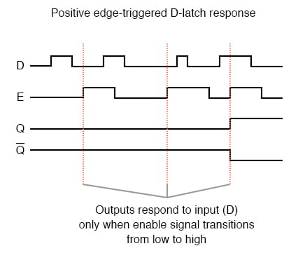
compare timing diagrams for a normal D latch versus one that is edge-triggered:
Implementing this timing function with semiconductor components is actually quite easy, as it exploits the inherent time delay within every logic gate (known as propagation delay). What we do is take an input signal and split it up two ways, then place a gate or a series of gates in one of those signal paths just to delay it a bit, then have both the original signal and its delayed counterpart enter into a two-input gate that outputs a high signal for the brief moment of time that the delayed signal has not yet caught up to the low-to-high change in the non-delayed signal. An example circuit for producing a clock pulse on a low-to-high input signal transition is shown here:
This circuit may be converted into a negative-edge pulse detector circuit with only a change of the final gate from AND to NOR:
The block symbols for flip-flops are slightly different from that of their respective latch counterparts:
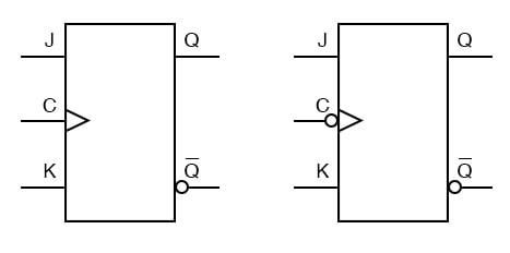
The triangle symbol next to the clock inputs tells us that these are edge-triggered devices, and consequently that these are flip-flops rather than latches. The symbols above are positive edge-triggered: that is, they “clock” on the rising edge (low-to-high transition) of the clock signal. Negative edge-triggered devices are symbolized with a bubble on the clock input line:
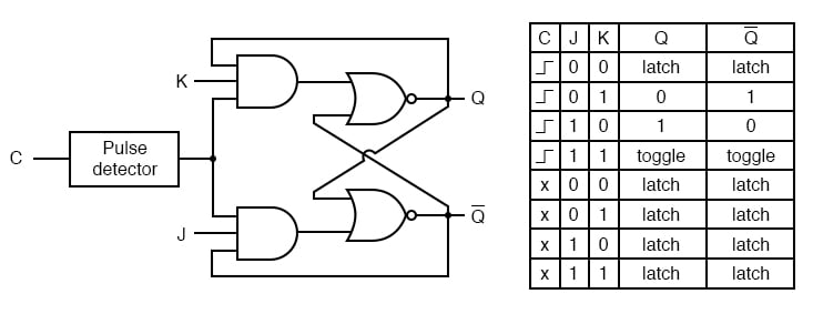
A flip-flop is a latch circuit with a “pulse detector” circuit connected to the enable (E) input, so that it is enabled only for a brief moment on either the rising or falling edge of a clock pulse.
Pulse detector circuits may be made from time-delay relays for ladder logic applications, or from semiconductor gates (exploiting the phenomenon of propagation delay).
J-K Flip-Flop
Another variation on a theme of bistable multivibrators is the J-K flip-flop. Essentially, this is a modified version of an S-R flip-flop with no “invalid” or “illegal” output state. Look closely at the following diagram to see how this is accomplished:
symbol
A J-K flip-flop is nothing more than an S-R flip-flop with an added layer of feedback. This feedback selectively enables one of the two set/reset inputs so that they cannot both carry an active signal to the multivibrator circuit, thus eliminating the invalid condition.
When both J and K inputs are activated, and the clock input is pulsed, the outputs (Q and not-Q) will swap states. That is, the circuit will toggle from a set state to a reset state or vice versa.
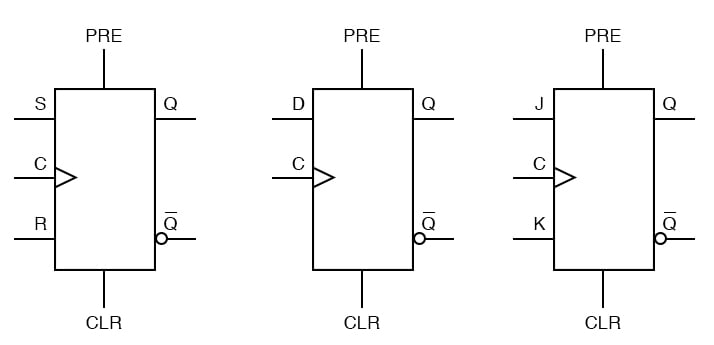
Asynchronous Flip-Flop Inputs
The normal data inputs to a flip flop (D, S and R, or J and K) are referred to as synchronous inputs because they have an effect on the outputs (Q and not-Q) only in step, or in sync, with the clock signal transitions.
These extra inputs that I now bring to your attention are called asynchronous because they can set or reset the flip-flop regardless of the status of the clock signal. Typically, they’re called preset and clear:
When the preset input is activated, the flip-flop will be set (Q=1, not-Q=0) regardless of any of the synchronous inputs or the clock. When the clear input is activated, the flip-flop will be reset (Q=0, not-Q=1), regardless of any of the synchronous inputs or the clock. So, what happens if both preset and clear inputs are activated? Surprise, surprise: we get an invalid state on the output, where Q and not-Q go to the same state, the same as our old friend, the S-R latch!
Asynchronous inputs on a flip-flop have control over the outputs (Q and not-Q) regardless of clock input status.
These inputs are called the preset (PRE) and clear (CLR). The preset input drives the flip-flop to a set state while the clear input drives it to a reset state.
It is possible to drive the outputs of a J-K flip-flop to an invalid condition using the asynchronous inputs, because all feedback within the multivibrator circuit is overridden.