How To Read Diodes Datasheet

Zener

Voltage Vz:   The Zener voltage or reverse voltage specification of the diode is often designated by the letters Vz.

Current :   The current, IZM, of a Zener diode is the maximum current that can flow through a Zener diode at its rated voltage, VZ.
Typically there is also a minimum current required for the operation of the diode. As a rough rule of thumb, this can be around 5 to 10 mA for a typical leaded 400 mW device. Below this current level, the diode does not break down adequately to maintain its stated voltage.
It is best to keep the Zener diode running above this minimum value with some margin, but without the likelihood of it dissipating too much power when the Zener needs to pass more current.

Power rating:   All Zener diodes have a power rating that should not be exceeded. This defines the maximum power that can be dissipated by the package, and it is the product of the voltage across the diode multiplied by the current flowing through it.

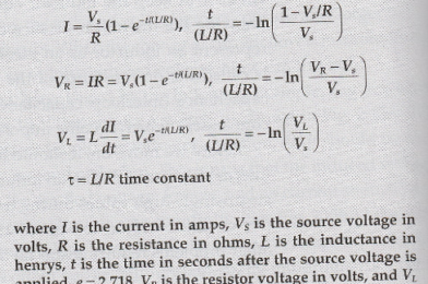
Zener resistance Rz:   The IV characteristic of the Zener diode is not completely vertical in the breakdown region. This means that for slight changes in current, there will be a small change in the voltage across the diode. The voltage change for a given change in current is the resistance of the diode. This value of resistance, often termed the resistance is designated Rz.

 Zener diode resistance shown as slope of breakdown area
Zener diode resistance

The inverse of the slope shown is referred to as the dynamic resistance of the diode, and this parameter is often noted in the manufacturers’ datasheets. Typically the slope does not vary much for different current levels, provided they are between about 0.1 and 1 times the rated current Izt.

Voltage tolerance:   With diodes being marked and sorted to meet the E12 or E24 value ranges, typical tolerance specifications for the diode are ±5%. Some datasheets may specify the voltage as a typical voltage and then provide a maximum and minimum.

How to use a Zener Diode

As said a Zener diode will mostly be used in a protection circuit or in a crude voltage regulator circuit. Either way, it very important to remember that a Zener diode should always be used along with a Zener resistor.

Zener resistor is nothing but an ordinary resistor which is used for current limiting purpose. This resistor decides (limits) the amount of current that can flow through the Zener diode or through the load connected to Zener diode; this was the Zener diode is protected from high current. If this resistor is not used the diode will be damaged due to high current. A simple Zener diode circuit is shown below.

Zener Diode Circuit

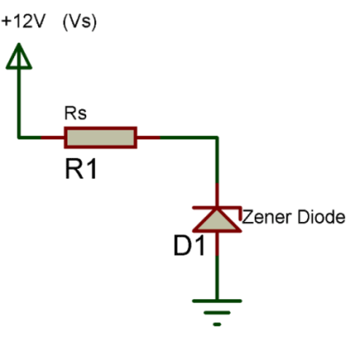
In the above circuit the formulae to calculate the Zener series resistor Rs is shown below

Rs = (Vs – Vz) / Iz

For a 1N4732A Zener diode the value of Vz is 4.7V and Pz is 500mW as mentioned in specifications above, now with supply voltage (Vs) of 12V the value of Rs will be

Rs = (12-4.7)/Iz
Iz = Pz/Vz = 500mW / 4.7V = ~106mA
Therefore, Rs = (12-4.7)/106 = 68 ohms
Rs = 68ohms (approx)

Diode 

Semiconductor material:
Silicon:   The forward turn on voltage is around 0.6V, which is high for some applications, although for Schottky diodes it is less.

Germanium:   Germanium is less widely used and but offers a low turn on voltage of around 0.2 to 0.3 V.

Diode type:  Zener diodes are used for providing reference voltages, whilst varactor diodes are used to provide a variable level of capacitance in an RF design according to the reverse bias provided. Rectifier diodes may use a straightforward PN junction diode, or in some cases they may use a Schottky diode for a lower forward voltage. Whatever the application is is necessary to use the right type of diode to obtain the required functionality and performance.

Forward voltage drop, Vf:   Any electronics device passing current will develop a resulting voltage across it and this diode characteristic is of great importance, especially for power rectification where power losses will be higher for a high forward voltage drop. Also diodes for RF designs often need a small forward voltage drop as signals may be small but still need to overcome it.

Reverse breakdown voltage, V(BR)R:   This is a little different to the peak inverse voltage in that this voltage is the point at which the diode will break down.

Maximum forward current If:   For an electronic circuit design that passes any levels of current it is necessary to ensure that the maximum current levels for the diode are not exceeded. As the current levels rise, so additional heat is dissipated and this needs to be removed.

Leakage current Ir:   If a perfect diode were available, then no current would flow when it was reverse biased. It is found that for a real PN junction diode, a very small amount of current flow in the reverse direction as a result of the minority carriers in the semiconductor. The level of leakage current is dependent upon three main factors. The reverse voltage is obviously significant. It is also temperature dependent, rising appreciably with temperature. It is also found that it is very dependent upon the type of semiconductor material used – silicon is very much better than germanium.

IV characteristic of a PN junction diode showing the reverse leakage current parameter
PN diode IV characteristic showing the leakage current parameter

The leakage current characteristic or specification for a PN junction diode is specified at a certain reverse voltage and particular temperature. The specification is normally defined in terms of in microamps, µA or picoamps, pA as the levels are normally very low before reverse breakdown occurs.

CHARACTERISTICTYPICAL VALUEUNITDETAILS
Max DC Blocking Voltage, Vr70V
Max forward continuous current, Ifm15mA
Reverse breakdown voltage, V(BR)R70V@ reverse current of 10µA
Reverse leakage current, IR200µAAt VR=50V
Forward voltage drop, VF0.41

1.00
Vat IF = 1.0 mA

IF=15mA
Junction capacitance, Cj2.0pFVR = 0V, f=1MHz
Reverse recovery time, trr1nS
1N5711 

How To Read Transistors Datasheet

Mosfets

Type of Control Channel: N Or P Channel
Vds : Maximum Drain-Source Voltage
Pd : Maximum Power Dissipation
Vgs : Maximum Gate-Source Voltage
Id : Maximum Drain Current
tr : Rise Time 0.01 ns for example
Cd : drain-source capacitance for example 600 pf
Rds : maximum drain-source on-state resistance 0.01 ohm for example

In a power MOSFET, the gate is insulated by a thin silicon oxide. Therefore, a power MOSFET has capacitances between the gate-drain, gate-source and drain-source terminals as shown in

BJT

Polarity: NPN
Pc : Maximum Collector Power Dissipation
Vcb : Maximum Collector-Base Voltage
Vce : Maximum Collector-Emitter Voltage
Veb : Maximum Emitter-Base Voltage
Ic : Maximum Collector Current
ft : Transition Frequency The transition frequency describes how the transistor’s current gain is affected by the input frequency. This is a low pass effect, so frequencies beyond 600 kHz on the original part or 4 MHz on the new one would start to be attenuated. Audible frequency range is 20 Hz – 20 kHz which is far below the transition frequency of both parts. No effects should be noticeable
Cc : Collector Capacitance
hfe : Forward Current Transfer Ratio

Inductors (LR + AC )

The LR Series Circuit

lr series circuit

The above LR series circuit is connected across a constant voltage source, (the battery) and a switch. Assume that the switch, S is open until it is closed at a time t = 0, and then remains permanently closed producing a “step response” type voltage input. The current, i begins to flow through the circuit but does not rise rapidly to its maximum value of Imax as determined by the ratio of V / R (Ohms Law).

This limiting factor is due to the presence of the self induced emf within the inductor as a result of the growth of magnetic flux, (Lenz’s Law). After a time the voltage source neutralizes the effect of the self induced emf, the current flow becomes constant and the induced current and field are reduced to zero.

We can use Kirchhoff’s Voltage Law, (KVL) to define the individual voltage drops that exist around the circuit and then hopefully use it to give us an expression for the flow of current.

Kirchhoff’s voltage law (KVL) gives us:

kirchhoffs voltage law

The voltage drop across the resistor, R is I*R (Ohms Law).

voltage drop across a resistor

The voltage drop across the inductor, L is by now our familiar expression L(di/dt)

voltage drop across an inductor

Then the final expression for the individual voltage drops around the LR series circuit can be given as:

lr series circuit voltage

We can see that the voltage drop across the resistor depends upon the current, i, while the voltage drop across the inductor depends upon the rate of change of the current, di/dt. When the current is equal to zero, ( i = 0 ) at time t = 0 the above expression, which is also a first order differential equation, can be rewritten to give the value of the current at any instant of time as:

Expression for the Current in an LR Series Circuit

current through lr series circuit
  • Where:
  •     V is in Volts
  •     R is in Ohms
  •     L is in Henries
  •     t is in Seconds
  •     e is the base of the Natural Logarithm = 2.71828

The Time Constant, ( τ ) of the LR series circuit is given as L/R and in which V/R represents the final steady state current value after five time constant values. Once the current reaches this maximum steady state value at 5τ, the inductance of the coil has reduced to zero acting more like a short circuit and effectively removing it from the circuit.

Therefore the current flowing through the coil is limited only by the resistive element in Ohms of the coils windings. A graphical representation of the current growth representing the voltage/time characteristics of the circuit can be presented as.

Transient Curves for an LR Series Circuit

lr transient curves

Since the voltage drop across the resistor, VR is equal to I*R (Ohms Law), it will have the same exponential growth and shape as the current. However, the voltage drop across the inductor, VL will have a value equal to:  Ve(-Rt/L). Then the voltage across the inductor, VL will have an initial value equal to the battery voltage at time t = 0 or when the switch is first closed and then decays exponentially to zero as represented in the above curves.

The time required for the current flowing in the LR series circuit to reach its maximum steady state value is equivalent to about 5 time constants or 5τ. This time constant τ, is measured by τ = L/R, in seconds, where R is the value of the resistor in ohms and L is the value of the inductor in Henries. This then forms the basis of an RL charging circuit were 5τ can also be thought of as “5*(L/R)” or the transient time of the circuit.

The transient time of any inductive circuit is determined by the relationship between the inductance and the resistance. For example, for a fixed value resistance the larger the inductance the slower will be the transient time and therefore a longer time constant for the LR series circuit. Likewise, for a fixed value inductance the smaller the resistance value the longer the transient time.

However, for a fixed value inductance, by increasing the resistance value the transient time and therefore the time constant of the circuit becomes shorter. This is because as the resistance increases the circuit becomes more and more resistive as the value of the inductance becomes negligible compared to the resistance. If the value of the resistance is increased sufficiently large compared to the inductance the transient time would effectively be reduced to almost zero.

LR Series Circuit Example No1

A coil which has an inductance of 40mH and a resistance of 2Ω is connected together to form a LR series circuit. If they are connected to a 20V DC supply.

a). What will be the final steady state value of the current.

lr series circuit steady state current

b) What will be the time constant of the RL series circuit.

time constant of lr series circuit

c) What will be the transient time of the RL series circuit.

transient time of lr series circuit

d) What will be the value of the induced emf after 10ms.

induced emf

e) What will be the value of the circuit current one time constant after the switch is closed.

instantaneous current

The Time Constant, τ of the circuit was calculated in question b) as being 20ms. Then the circuit current at this time is given as:

instantaneous current value

You may have noticed that the answer for question (e) which gives a value of 6.32 Amps at one time constant, is equal to 63.2% of the final steady state current value of 10 Amps we calculated in question (a). This value of 63.2% or 0.632 x IMAX also corresponds with the transient curves shown above.

Power in an LR Series Circuit

Then from above, the instantaneous rate at which the voltage source delivers power to the circuit is given as:

instantaneous power

The instantaneous rate at which power is dissipated by the resistor in the form of heat is given as:

power in resistor

The rate at which energy is stored in the inductor in the form of magnetic potential energy is given as:

power in inductor

Then we can find the total power in a RL series circuit by multiplying by i and is therefore:

instantaneous power in a lr series circuit

Where the first I2R term represents the power dissipated by the resistor in heat, and the second term represents the power absorbed by the inductor, its magnetic energy.

AC Inductor Phasor Diagram

inductor phase diagram

These voltage and current waveforms show that for a purely inductive circuit the current lags the voltage by 90o. Likewise, we can also say that the voltage leads the current by 90o. Either way the general expression is that the current lags as shown in the vector diagram. Here the current vector and the voltage vector are shown displaced by 90oThe current lags the voltage.

We can also write this statement as, VL = 0o and IL = -90o with respect to the voltage, VL. If the voltage waveform is classed as a sine wave then the current, IL can be classed as a negative cosine and we can define the value of the current at any point in time as being:

instantaneous inductor current

Where: ω is in radians per second and t is in seconds.

Since the current always lags the voltage by 90o in a purely inductive circuit, we can find the phase of the current by knowing the phase of the voltage or vice versa. So if we know the value of VL, then IL must lag by 90o. Likewise, if we know the value of IL then VL must therefore lead by 90o. Then this ratio of voltage to current in an inductive circuit will produce an equation that defines the Inductive ReactanceXL of the coil.

Inductive Reactance

inductive reactance

We can rewrite the above equation for inductive reactance into a more familiar form that uses the ordinary frequency of the supply instead of the angular frequency in radians, ω and this is given as:

inductive reactance equation

Where: ƒ is the Frequency and L is the Inductance of the Coil and 2πƒ = ω.

From the above equation for inductive reactance, it can be seen that if either of the Frequency or Inductance was increased the overall inductive reactance value would also increase. As the frequency approaches infinity the inductors reactance would also increase to infinity acting like an open circuit.

However, as the frequency approaches zero or DC, the inductors reactance would decrease to zero, acting like a short circuit. This means then that inductive reactance is “proportional” to frequency.

In other words, inductive reactance increases with frequency resulting in XL being small at low frequencies and XL being high at high frequencies and this demonstrated in the following graph:

Inductive Reactance against Frequency

reactance against frequencyThe slope shows that the “Inductive Reactance” of an inductor increases as the supply frequency across it increases.Therefore Inductive Reactance is proportional to frequency giving: ( XL α ƒ )

Then we can see that at DC an inductor has zero reactance (short-circuit), at high frequencies an inductor has infinite reactance (open-circuit).