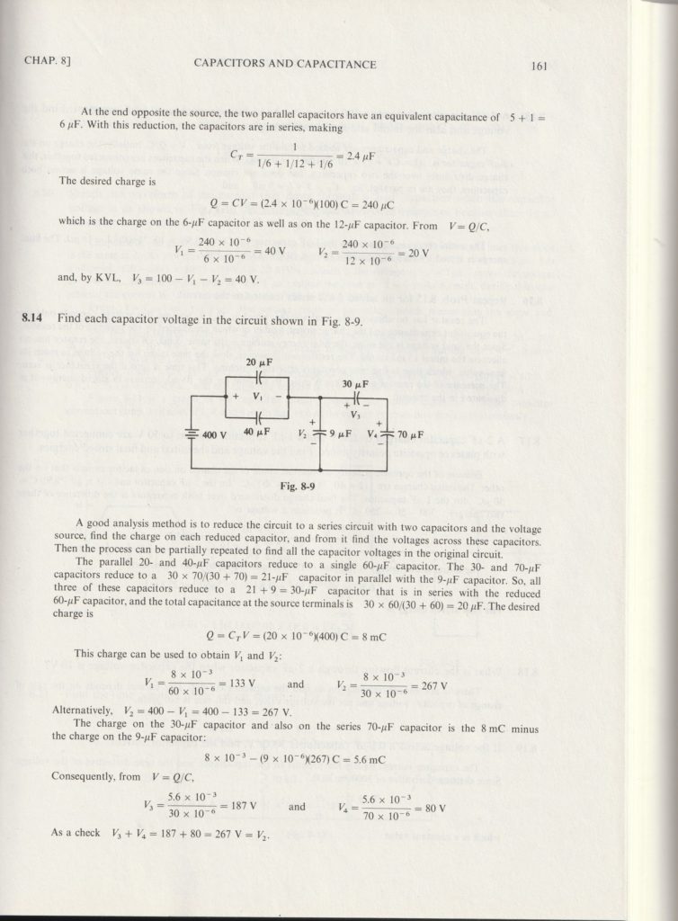
The most common amplifier configuration for an NPN transistor is that of the Common Emitter Amplifier circuit
All types of transistor amplifiers operate using AC signal inputs which alternate between a positive value and a negative value so some way of “presetting” the amplifier circuit to operate between these two maximum or peak values is required. This is achieved using a process known as Biasing. Biasing is very important in amplifier design as it establishes the correct operating point of the transistor amplifier ready to receive signals, thereby reducing any distortion to the output signal.
We also saw that a static or DC load line can be drawn onto these output characteristics curves to show all the possible operating points of the transistor from fully “ON” to fully “OFF”, and to which the quiescent operating point or Q-point of the amplifier can be found.
The aim of any small signal amplifier is to amplify all of the input signal with the minimum amount of distortion possible to the output signal, in other words, the output signal must be an exact reproduction of the input signal but only bigger (amplified).
To obtain low distortion when used as an amplifier the operating quiescent point needs to be correctly selected. This is in fact the DC operating point of the amplifier and its position may be established at any point along the load line by a suitable biasing arrangement.
The best possible position for this Q-point is as close to the center position of the load line as reasonably possible, thereby producing a Class A type amplifier operation, ie. Vce = 1/2Vcc. Consider the Common Emitter Amplifier circuit shown below.
The Common Emitter Amplifier Circuit
The single stage common emitter amplifier circuit shown above uses what is commonly called “Voltage Divider Biasing”. This type of biasing arrangement uses two resistors as a potential divider network across the supply with their center point supplying the required Base bias voltage to the transistor. Voltage divider biasing is commonly used in the design of bipolar transistor amplifier circuits.
This method of biasing the transistor greatly reduces the effects of varying Beta, ( β ) by holding the Base bias at a constant steady voltage level allowing for best stability. The quiescent Base voltage (Vb) is determined by the potential divider network formed by the two resistors, R1, R2 and the power supply voltage Vcc as shown with the current flowing through both resistors.
Then the total resistance RT will be equal to R1 + R2 giving the current as i = Vcc/RT. The voltage level generated at the junction of resistors R1 and R2 holds the Base voltage (Vb) constant at a value below the supply voltage.
Then the potential divider network used in the common emitter amplifier circuit divides the supply voltage in proportion to the resistance. This bias reference voltage can be easily calculated using the simple voltage divider formula below:
Transistor Bias Voltage
The same supply voltage, (Vcc) also determines the maximum Collector current, Ic when the transistor is switched fully “ON” (saturation), Vce = 0. The Base current Ib for the transistor is found from the Collector current, Ic and the DC current gain Beta, β of the transistor.
Beta Value
Beta is sometimes referred to as hFE which is the transistors forward current gain in the common emitter configuration. Beta has no units as it is a fixed ratio of the two currents, Ic and Ib so a small change in the Base current will cause a large change in the Collector current.
One final point about Beta. Transistors of the same type and part number will have large variations in their Beta value. For example, the BC107 NPN Bipolar transistor has a DC current gain Beta value of between 110 and 450 (data sheet value). So one BC107 may have a Beta value of 110, while another one may have a Beta value of 450, but they are both BC107 npn transistors. This is because Beta is a characteristic of the transistors construction and not of its operation.
As the Base/Emitter junction is forward-biased, the Emitter voltage, Ve will be one junction voltage drop different to the Base voltage. If the voltage across the Emitter resistor is known then the Emitter current, Ie can be easily calculated using Ohm’s Law. The Collector current, Ic can be approximated, since it is almost the same value as the Emitter current.
Common Emitter Amplifier Example No1
An common emitter amplifier circuit has a load resistance, RL of 1.2kΩ and a supply voltage of 12v. Calculate the maximum Collector current (Ic) flowing through the load resistor when the transistor is switched fully “ON” (saturation), assume Vce = 0. Also find the value of the Emitter resistor, RE if it has a voltage drop of 1v across it. Calculate the values of all the other circuit resistors assuming a standard NPN silicon transistor.
This then establishes point “A” on the Collector current vertical axis of the characteristics curves and occurs when Vce = 0. When the transistor is switched fully “OFF”, their is no voltage drop across either resistor RE or RL as no current is flowing through them. Then the voltage drop across the transistor, Vce is equal to the supply voltage, Vcc. This establishes point “B” on the horizontal axis of the characteristics curves.
Generally, the quiescent Q-point of the amplifier is with zero input signal applied to the Base, so the Collector sits about half-way along the load line between zero volts and the supply voltage, (Vcc/2). Therefore, the Collector current at the Q-point of the amplifier will be given as:
This static DC load line produces a straight line equation whose slope is given as: -1/(RL + RE) and that it crosses the vertical Ic axis at a point equal to Vcc/(RL + RE). The actual position of the Q-point on the DC load line is determined by the mean value of Ib.
As the Collector current, Ic of the transistor is also equal to the DC gain of the transistor (Beta), times the Base current (β*Ib), if we assume a Beta (β) value for the transistor of say 100, (one hundred is a reasonable average value for low power signal transistors) the Base current Ib flowing into the transistor will be given as:
Instead of using a separate Base bias supply, it is usual to provide the Base Bias Voltage from the main supply rail (Vcc) through a dropping resistor, R1. Resistors, R1 and R2 can now be chosen to give a suitable quiescent Base current of 45.8μA or 46μA rounded off to the nearest integer. The current flowing through the potential divider circuit has to be large compared to the actual Base current, Ib, so that the voltage divider network is not loaded by the Base current flow.
A general rule of thumb is a value of at least 10 times Ib flowing through the resistor R2. Transistor Base/Emitter voltage, Vbe is fixed at 0.7V (silicon transistor) then this gives the value of R2 as:
If the current flowing through resistor R2 is 10 times the value of the Base current, then the current flowing through resistor R1 in the divider network must be 11 times the value of the Base current. That is: IR2 + Ib.
Thus the voltage across resistor R1 is equal to Vcc – 1.7v (VRE + 0.7 for silicon transistor) which is equal to 10.3V, therefore R1 can be calculated as:
The value of the Emitter resistor, RE can be easily calculated using Ohm’s Law. The current flowing through RE is a combination of the Base current, Ib and the Collector current Ic and is given as:
Resistor, RE is connected between the transistors Emitter terminal and ground, and we said previously that there is a voltage drop of 1 volt across it. Thus the value of the Emitter resistor, RE is calculated as:
So, for our example above, the preferred values of the resistors chosen to give a tolerance of 5% (E24) are:
Then, our original Common Emitter Amplifier circuit above can be rewritten to include the values of the components that we have just calculated above.
Completed Common Emitter Circuit
Amplifier Coupling Capacitors
In Common Emitter Amplifier circuits, capacitors C1 and C2 are used as Coupling Capacitors to separate the AC signals from the DC biasing voltage. This ensures that the bias condition set up for the circuit to operate correctly is not affected by any additional amplifier stages, as the capacitors will only pass AC signals and block any DC component. The output AC signal is then superimposed on the biasing of the following stages. Also a bypass capacitor, CE is included in the Emitter leg circuit.
This capacitor is effectively an open circuit component for DC biasing conditions, which means that the biasing currents and voltages are not affected by the addition of the capacitor maintaining a good Q-point stability.
However, this parallel connected bypass capacitor effectively becomes a short circuit to the Emitter resistor at high frequency signals due to its reactance. Thus only RL plus a very small internal resistance acts as the transistors load increasing voltage gain to its maximum. Generally, the value of the bypass capacitor, CE is chosen to provide a reactance of at most, 1/10th the value of RE at the lowest operating signal frequency.
Output Characteristics Curves
Ok, so far so good. We can now construct a series of curves that show the Collector current, Ic against the Collector/Emitter voltage, Vce with different values of Base current, Ib for our simple common emitter amplifier circuit.
These curves are known as the “Output Characteristic Curves” and are used to show how the transistor will operate over its dynamic range. A static or DC load line is drawn onto the curves for the load resistor RL of 1.2kΩ to show all the transistors possible operating points.
When the transistor is switched “OFF”, Vce equals the supply voltage Vcc and this is point “B” on the line. Likewise when the transistor is fully “ON” and saturated the Collector current is determined by the load resistor, RL and this is point “A” on the line.
We calculated before from the DC gain of the transistor that the Base current required for the mean position of the transistor was 45.8μA and this is marked as point Q on the load line which represents the Quiescent point or Q-point of the amplifier. We could quite easily make life easy for ourselves and round off this value to 50μA exactly, without any effect to the operating point.
Output Characteristics Curves
Point Q on the load line gives us the Base current Q-point of Ib = 45.8μA or 46μA. We need to find the maximum and minimum peak swings of Base current that will result in a proportional change to the Collector current, Ic without any distortion to the output signal.
As the load line cuts through the different Base current values on the DC characteristics curves we can find the peak swings of Base current that are equally spaced along the load line. These values are marked as points “N” and “M” on the line, giving a minimum and a maximum Base current of 20μA and 80μA respectively.
These points, “N” and “M” can be anywhere along the load line that we choose as long as they are equally spaced from Q. This then gives us a theoretical maximum input signal to the Base terminal of 60μA peak-to-peak, (30μA peak) without producing any distortion to the output signal.
Any input signal giving a Base current greater than this value will drive the transistor to go beyond point “N” and into its “cut-off” region or beyond point “M” and into its Saturation region thereby resulting in distortion to the output signal in the form of “clipping”.
Using points “N” and “M” as an example, the instantaneous values of Collector current and corresponding values of Collector-emitter voltage can be projected from the load line. It can be seen that the Collector-emitter voltage is in anti-phase (–180o) with the collector current.
As the Base current Ib changes in a positive direction from 50μA to 80μA, the Collector-emitter voltage, which is also the output voltage decreases from its steady state value of 5.8 volts to 2.0 volts.
Then a single stage Common Emitter Amplifier is also an “Inverting Amplifier” as an increase in Base voltage causes a decrease in Vout and a decrease in Base voltage produces an increase in Vout. In other words the output signal is 180o out-of-phase with the input signal.
Common Emitter Voltage Gain
The Voltage Gain of the common emitter amplifier is equal to the ratio of the change in the input voltage to the change in the amplifiers output voltage. Then ΔVL is Vout and ΔVB is Vin. But voltage gain is also equal to the ratio of the signal resistance in the Collector to the signal resistance in the Emitter and is given as:
We mentioned earlier that as the signal frequency increases the bypass capacitor, CE starts to short out the Emitter resistor due to its reactance. Then at high frequencies RE = 0, making the gain infinite.
However, bipolar transistors have a small internal resistance built into their Emitter region called Re. The transistors semiconductor material offers an internal resistance to the flow of current through it and is generally represented by a small resistor symbol shown inside the main transistor symbol.
Transistor data sheets tell us that for a small signal bipolar transistors this internal resistance is the product of 25mV ÷ Ie (25mV being the internal volt drop across the Emitter junction layer), then for our common Emitter amplifier circuit above this resistance value will be equal to:
This internal Emitter leg resistance will be in series with the external Emitter resistor, RE, then the equation for the transistors actual gain will be modified to include this internal resistance so will be:
At low frequency signals the total resistance in the Emitter leg is equal to RE + Re. At high frequency, the bypass capacitor shorts out the Emitter resistor leaving only the internal resistance Re in the Emitter leg resulting in a high gain. Then for our common emitter amplifier circuit above, the gain of the circuit at both low and high signal frequencies is given as:
Gain at Low Frequencies
Gain at High Frequencies
One final point, the voltage gain is dependent only on the values of the Collector resistor, RL and the Emitter resistance, (RE + Re) it is not affected by the current gain Beta, β (hFE) of the transistor.
So, for our simple example above we can now summarise all the values we have calculated for our common emitter amplifier circuit and these are:
Minimum
Mean
Maximum
Base Current
20μA
50μA
80μA
Collector Current
2.0mA
4.8mA
7.7mA
Output Voltage Swing
2.0V
5.8V
9.3V
Amplifier Gain
-5.32
-218
Common Emitter Amplifier Summary
Then to summarise. The Common Emitter Amplifier circuit has a resistor in its Collector circuit. The current flowing through this resistor produces the voltage output of the amplifier. The value of this resistor is chosen so that at the amplifiers quiescent operating point, Q-point this output voltage lies half way along the transistors load line.
The Base of the transistor used in a common emitter amplifier is biased using two resistors as a potential divider network. This type of biasing arrangement is commonly used in the design of bipolar transistor amplifier circuits and greatly reduces the effects of varying Beta, ( β ) by holding the Base bias at a constant steady voltage. This type of biasing produces the greatest stability.
A resistor can be included in the emitter leg in which case the voltage gain becomes -RL/RE. If there is no external Emitter resistance, the voltage gain of the amplifier is not infinite as there is a very small internal resistance, Re in the Emitter leg. The value of this internal resistance is equal to 25mV/IE
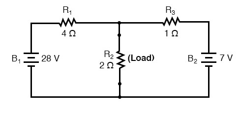
Norton’s Theorem states that it is possible to simplify any linear circuit, no matter how complex, to an equivalent circuit with just a single current source and parallel resistance connected to a load. Just as with Thevenin’s Theorem, the qualification of “linear” is identical to that found in the Superposition Theorem: all underlying equations must be linear (no exponents or roots).
Simplifying Linear Circuits
Contrasting our original example circuit against the Norton equivalent: it looks something like this:
. . . after Norton conversion . . .
Remember that a current source is a component whose job is to provide a constant amount of current, outputting as much or as little voltage necessary to maintain that constant current.
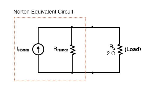
Thevenin’s Theorem vs. Norton’s Theorem
As with Thevenin’s Theorem, everything in the original circuit except the load resistance has been reduced to an equivalent circuit that is simpler to analyze. Also similar to Thevenin’s Theorem are the steps used in Norton’s Theorem to calculate the Norton source current (INorton) and Norton resistance (RNorton).
Identify The Load Resistance
As before, the first step is to identify the load resistance and remove it from the original circuit:
Find The Norton Current
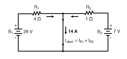
Then, to find the Norton current (for the current source in the Norton equivalent circuit), place a direct wire (short) connection between the load points and determine the resultant current. Note that this step is exactly opposite the respective step in Thevenin’s Theorem, where we replaced the load resistor with a break (open circuit):
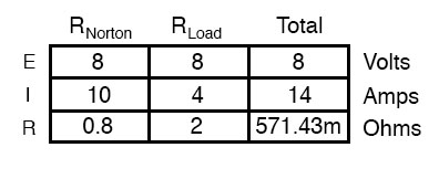
With zero voltage dropped between the load resistor connection points, the current through R1 is strictly a function of B1‘s voltage and R1‘s resistance: 7 amps (I=E/R). Likewise, the current through R3 is now strictly a function of B2‘s voltage and R3‘s resistance: 7 amps (I=E/R). The total current through the short between the load connection points is the sum of these two currents: 7 amps + 7 amps = 14 amps. This figure of 14 amps becomes the Norton source current (INorton) in our equivalent circuit:
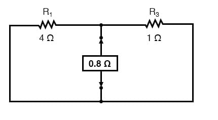
Find Norton Resistance
Remember, the arrow notation for current source points in the direction of conventional current flow. To calculate the Norton resistance (RNorton), we do the exact same thing as we did for calculating Thevenin resistance (RThevenin): take the original circuit (with the load resistor still removed), remove the power sources (in the same style as we did with the Superposition Theorem: voltage sources replaced with wires and current sources replaced with breaks), and figure total resistance from one load connection point to the other:
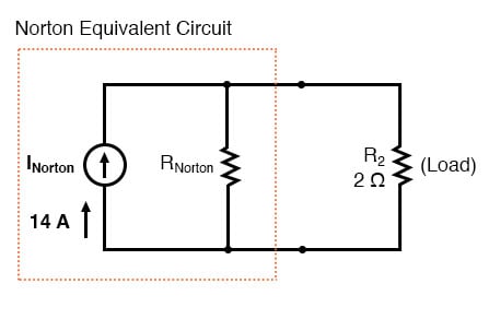
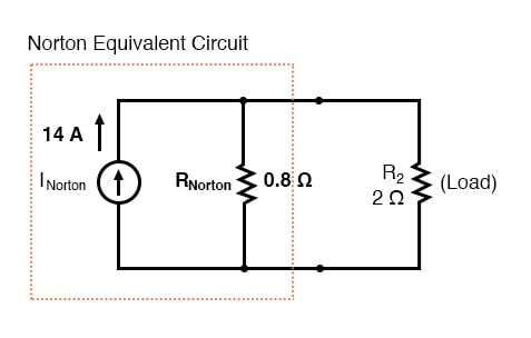
Now our Norton equivalent circuit looks like this:
Determine The Voltage Across The Load Resistor
If we re-connect our original load resistance of 2 Ω, we can analyze the Norton circuit as a simple parallel arrangement:
As with the Thevenin equivalent circuit, the only useful information from this analysis is the voltage and current values for R2; the rest of the information is irrelevant to the original circuit. However, the same advantages seen with Thevenin’s Theorem apply to Norton’s as well: if we wish to analyze load resistor voltage and current over several different values of load resistance, we can use the Norton equivalent circuit, again and again, applying nothing more complex than simple parallel circuit analysis to determine what’s happening with each trial load.
proof
REVIEW:
Norton’s Theorem is a way to reduce a network to an equivalent circuit composed of a single current source, parallel resistance, and parallel load.
Steps to follow for Norton’s Theorem:
Find the Norton source current by removing the load resistor from the original circuit and calculating the current through a short (wire) jumping across the open connection points where the load resistor used to be.
Find the Norton resistance by removing all power sources in the original circuit (voltage sources shorted and current sources open) and calculating total resistance between the open connection points.
Draw the Norton equivalent circuit, with the Norton current source in parallel with the Norton resistance. The load resistor re-attaches between the two open points of the equivalent circuit.
Analyze voltage and current for the load resistor following the rules for parallel circuits.
Superposition theorem is one of those strokes of genius that takes a complex subject and simplifies it in a way that makes perfect sense. A theorem like Millman’s certainly works well, but it is not quite obvious why it works so well. Superposition, on the other hand, is obvious.
Series/Parallel Analysis
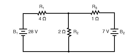
The strategy used in the Superposition Theorem is to eliminate all but one source of power within a network at a time, using series/parallel analysis to determine voltage drops (and/or currents) within the modified network for each power source separately. Then, once voltage drops and/or currents have been determined for each power source working separately, the values are all “superimposed” on top of each other (added algebraically) to find the actual voltage drops/currents with all sources active. Let’s look at our example circuit again and apply Superposition Theorem to it:
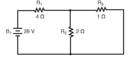
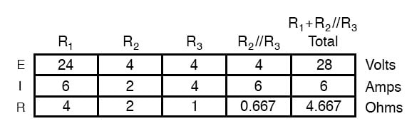
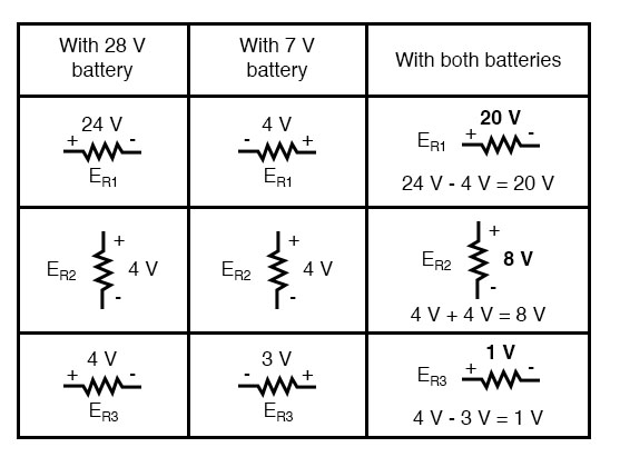
Since we have two sources of power in this circuit, we will have to calculate two sets of values for voltage drops and/or currents, one for the circuit with only the 28-volt battery in effect. . .
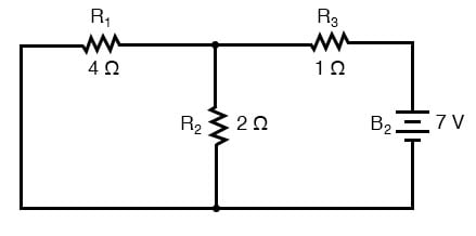
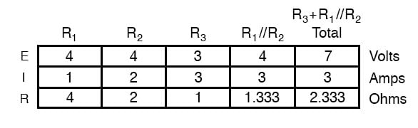
. . . and one for the circuit with only the 7-volt battery in effect:
When re-drawing the circuit for series/parallel analysis with one source, all other voltage sources are replaced by wires (shorts), and all current sources with open circuits (breaks). Since we only have voltage sources (batteries) in our example circuit, we will replace every inactive source during analysis with a wire.
Analyzing the circuit with only the 28-volt battery, we obtain the following values for voltage and current:
Analyzing the circuit with only the 7-volt battery, we obtain another set of values for voltage and current:
By Superimposing
When superimposing these values of voltage and current, we have to be very careful to consider polarity (of the voltage drop) and direction (of the current flow), as the values have to be added algebraically.
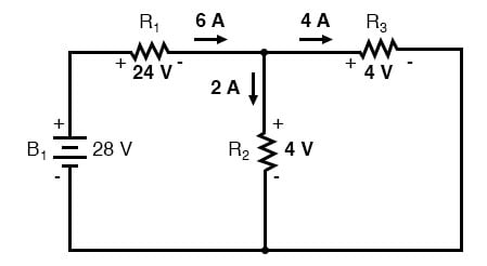
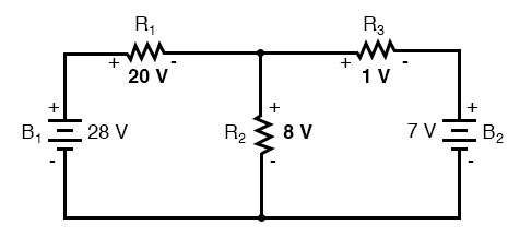
Applying these superimposed voltage figures to the circuit, the end result looks something like this:
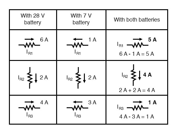
Currents add up algebraically as well and can either be superimposed as done with the resistor voltage drops or simply calculated from the final voltage drops and respective resistances (I=E/R). Either way, the answers will be the same. Here I will show the superposition method applied to current:
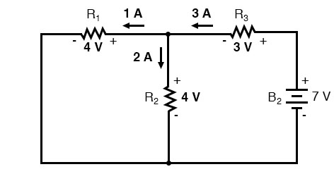
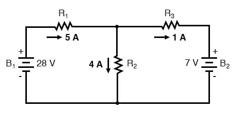
Once again applying these superimposed figures to our circuit:
Prerequisites for the Superposition Theorem
Quite simple and elegant, don’t you think? It must be noted, though, that the Superposition Theorem works only for circuits that are reducible to series/parallel combinations for each of the power sources at a time (thus, this theorem is useless for analyzing an unbalanced bridge circuit), and it only works where the underlying equations are linear (no mathematical powers or roots). The requisite of linearity means that Superposition Theorem is only applicable for determining voltage and current, not power!!! Power dissipations, being nonlinear functions, do not algebraically add to an accurate total when only one source is considered at a time. The need for linearity also means this Theorem cannot be applied in circuits where the resistance of a component changes with voltage or current. Hence, networks containing components like lamps (incandescent or gas-discharge) or varistors could not be analyzed.
Another prerequisite for Superposition Theorem is that all components must be “bilateral,” meaning that they behave the same with electrons flowing in either direction through them. Resistors have no polarity-specific behavior, and so the circuits we’ve been studying so far all meet this criterion.
The Superposition Theorem finds use in the study of alternating current (AC) circuits, and semiconductor (amplifier) circuits, where sometimes AC is often mixed (superimposed) with DC. Because AC voltage and current equations (Ohm’s Law) are linear just like DC, we can use Superposition to analyze the circuit with just the DC power source, then just the AC power source, combining the results to tell what will happen with both AC and DC sources in effect. For now, though, Superposition will suffice as a break from having to do simultaneous equations to analyze a circuit.
REVIEW:
The Superposition Theorem states that a circuit can be analyzed with only one source of power at a time, the corresponding component voltages and currents algebraically added to find out what they’ll do with all power sources in effect.
To negate all but one power source for analysis, replace any source of voltage (batteries) with a wire; replace any current source with an open (break).
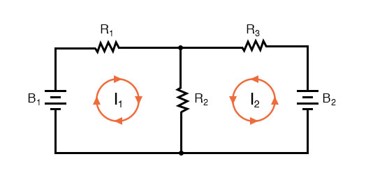
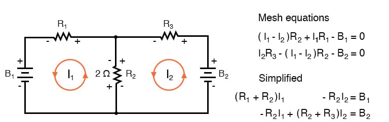
The Mesh-Current Method, also known as the Loop Current Method, is quite similar to the Branch Current method in that it uses simultaneous equations, Kirchhoff’s Voltage Law, and Ohm’s Law to determine unknown currents in a network. It differs from the Branch Current method in that it does not use Kirchhoff’s Current Law, and it is usually able to solve a circuit with less unknown variables and less simultaneous equations, which is especially nice if you’re forced to solve without a calculator.
Mesh Current, conventional method
Let’s see how this method works on the same example problem:
Identify Loops
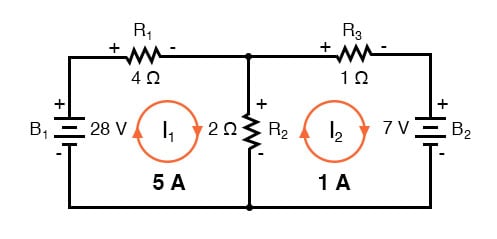
The first step in the Mesh Current method is to identify “loops” within the circuit encompassing all components. In our example circuit, the loop formed by B1, R1, and R2 will be the first while the loop formed by B2, R2, and R3 will be the second. The strangest part of the Mesh Current method is envisioning circulating currents in each of the loops. In fact, this method gets its name from the idea of these currents meshing together between loops like sets of spinning gears:
The choice of each current’s direction is entirely arbitrary, just as in the Branch Current method, but the resulting equations are easier to solve if the currents are going the same direction through intersecting components (note how currents I1 and I2 are both going “up” through resistor R2, where they “mesh,” or intersect). If the assumed direction of a mesh current is wrong, the answer for that current will have a negative value.
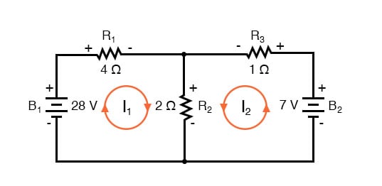
Label the Voltage Drop Polarities
The next step is to label all voltage drop polarities across resistors according to the assumed directions of the mesh currents. Remember that the “upstream” end of a resistor will always be negative, and the “downstream” end of a resistor positive with respect to each other, since electrons are negatively charged. The battery polarities, of course, are dictated by their symbol orientations in the diagram, and may or may not “agree” with the resistor polarities (assumed current directions):
Using Kirchhoff’s Voltage Law, we can now step around each of these loops, generating equations representative of the component voltage drops and polarities. As with the Branch Current method, we will denote a resistor’s voltage drop as the product of the resistance (in ohms) and its respective mesh current (that quantity being unknown at this point). Where two currents mesh together, we will write that term in the equation with resistor current being the sum of the two meshing currents.
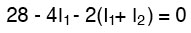
Tracing the Left Loop of the Circuit with Equations
Tracing the left loop of the circuit, starting from the upper-left corner and moving counter-clockwise (the choice of starting points and directions is ultimately irrelevant), counting polarity as if we had a voltmeter in hand, red lead on the point ahead and black lead on the point behind, we get this equation:
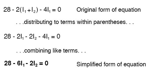
Notice that the middle term of the equation uses the sum of mesh currents I1 and I2 as the current through resistor R2. This is because mesh currents I1 and I2 are going the same direction through R2, and thus complement each other. Distributing the coefficient of 2 to the I1 and I2 terms, and then combining I1 terms in the equation, we can simplify as such:
At this time we have one equation with two unknowns. To be able to solve for two unknown mesh currents, we must have two equations. If we trace the other loop of the circuit, we can obtain another KVL equation and have enough data to solve for the two currents. Creature of habit that I am, I’ll start at the upper-left-hand corner of the right loop and trace counter-clockwise:
Simplifying the equation as before, we end up with:
Solving For The Unknown
Now, with two equations, we can use one of several methods to mathematically solve for the unknown currents I1 and I2:
Redraw Circuit
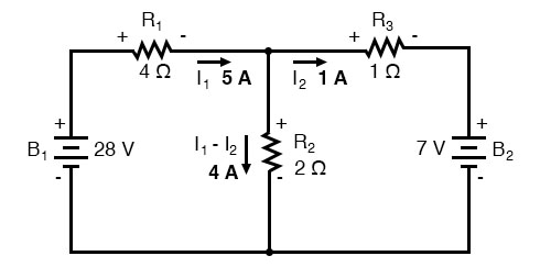
Knowing that these solutions are values for mesh currents, not branch currents, we must go back to our diagram to see how they fit together to give currents through all components:
The solution of -1 amp for I2 means that we initially assumed the direction of current was incorrect. In actuality, I2 is flowing in a counter-clockwise direction at a value of (positive) 1 amp:
This change of current direction from what was first assumed will alter the polarity of the voltage drops across R2 and R3 due to current I2. From here, we can say that the current through R1 is 5 amps, with the voltage drop across R1 being the product of current and resistance (E=IR), 20 volts (positive on the left and negative on the right).
Also, we can safely say that the current through R3 is 1 amp, with a voltage drop of 1 volt (E=IR), positive on the left and negative on the right. But what is happening at R2?
Mesh current I1 is going “down” through R2, while mesh current I2 is going “up” through R2. To determine the actual current through R2, we must see how mesh currents I1 and I2 interact (in this case they’re in opposition), and algebraically add them to arrive at a final value. Since I1 is going “down” at 5 amps, and I2 is going “up” at 1 amp, the real current through R2 must be a value of 4 amps, going “down”:
A current of 4 amps through R2‘s resistance of 2 Ω gives us a voltage drop of 8 volts (E=IR), positive on the top and negative on the bottom.
Advantage of Mesh Current Analysis
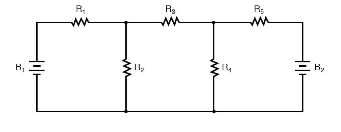
The primary advantage of Mesh Current analysis is that it generally allows for the solution of a large network with fewer unknown values and fewer simultaneous equations. Our example problem took three equations to solve the Branch Current method and only two equations using the Mesh Current method. This advantage is much greater as networks increase in complexity:
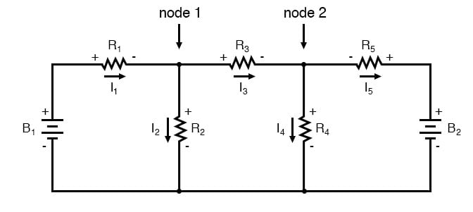
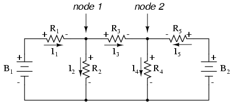
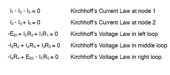
To solve this network using Branch Currents, we’d have to establish five variables to account for each and every unique current in the circuit (I1 through I5). This would require five equations for the solution, in the form of two KCL equations and three KVL equations (two equations for KCL at the nodes, and three equations for KVL in each loop):
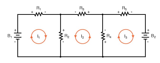
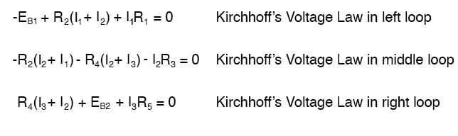
I suppose if you have nothing better to do with your time than to solve for five unknown variables with five equations, you might not mind using the Branch Current method of analysis for this circuit. For those of us who have better things to do with our time, the Mesh Current method is a whole lot easier, requiring only three unknowns and three equations to solve:
Less equations to work with is a decided advantage, especially when performing a simultaneous equation solution by hand (without a calculator).
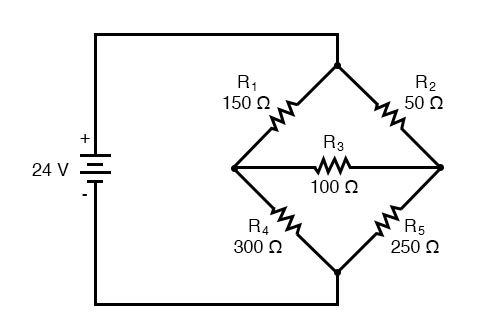
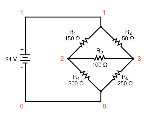
Unbalanced Wheatstone Bridge
Another type of circuit that lends itself well to Mesh Current is the unbalanced Wheatstone Bridge. Take this circuit, for example:
Since the ratios of R1/R4 and R2/R5 are unequal, we know that there will be the voltage across resistor R3, and some amount of current through it. As discussed at the beginning of this chapter, this type of circuit is irreducible by normal series-parallel analysis, and may only be analyzed by some other method.
We could apply the Branch Current method to this circuit, but it would require six currents (I1 through I6), leading to a very large set of simultaneous equations to solve. Using the Mesh Current method, though, we may solve for all currents and voltages with much fewer variables.
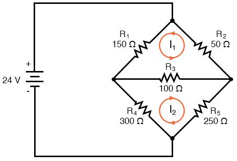
Draw Mesh
The first step in the Mesh Current method is to draw just enough mesh currents to account for all components in the circuit. Looking at our bridge circuit, it should be obvious where to place two of these currents:
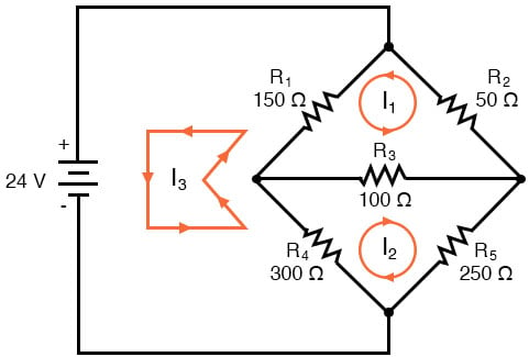
The directions of these mesh currents, of course, is arbitrary. However, two mesh currents are not enough in this circuit, because neither I1 nor I2 goes through the battery. So, we must add a third mesh current, I3:
Here, I have chosen I3 to loop from the bottom side of the battery, through R4, through R1, and back to the top side of the battery. This is not the only path I could have chosen for I3, but it seems the simplest.
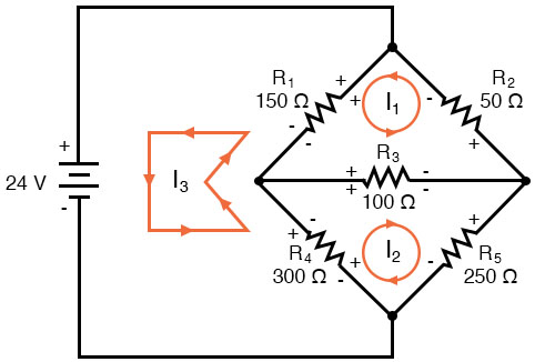
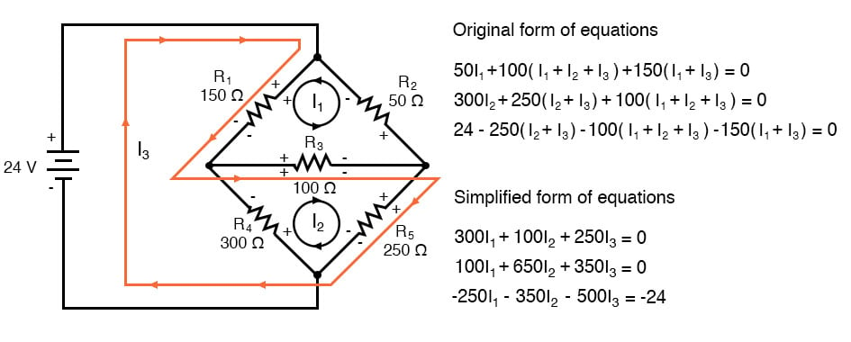
Label The Resistor Voltage Drop Polarities
Now, we must label the resistor voltage drop polarities, following each of the assumed currents’ directions:
Notice something very important here: at resistor R4, the polarities for the respective mesh currents do not agree. This is because those mesh currents (I2 and I3) are going through R4 in different directions. This does not preclude the use of the Mesh Current method of analysis, but it does complicate it a bit. Though later, we will show how to avoid the R4 current clash. (See Example below)
Using KVL
Generating a KVL equation for the top loop of the bridge, starting from the top node and tracing in a clockwise direction:
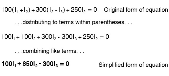
In this equation, we represent the common directions of currents by their sums through common resistors. For example, resistor R3, with a value of 100 Ω, has its voltage drop represented in the above KVL equation by the expression 100(I1 + I2), since both currents I1 and I2 go through R3 from right to left. The same may be said for resistor R1, with its voltage drop expression shown as 150(I1 + I3), since both I1 and I3 go from bottom to top through that resistor, and thus work together to generate its voltage drop.
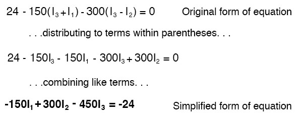
Generating a KVL equation for the bottom loop of the bridge will not be so easy since we have two currents going against each other through resistor R4. Here is how I do it (starting at the right-hand node, and tracing counter-clockwise):
Note how the second term in the equation’s original form has resistor R4‘s value of 300 Ω multiplied by the difference between I2 and I3 (I2 – I3). This is how we represent the combined effect of two mesh currents going in opposite directions through the same component. Choosing the appropriate mathematical signs is very important here: 300(I2 – I3) does not mean the same thing as 300(I3 – I2). I chose to write 300(I2 – I3) because I was thinking first of I2‘s effect (creating a positive voltage drop, measuring with an imaginary voltmeter across R4, red lead on the bottom and black lead on the top), and secondarily of I3‘s effect (creating a negative voltage drop, red lead on the bottom and black lead on the top). If I had thought in terms of I3‘s effect first and I2‘s effect secondarily, holding my imaginary voltmeter leads in the same positions (red on the bottom and black on top), the expression would have been -300(I3 – I2). Note that this expression is mathematically equivalent to the first one: +300(I2 – I3).
Well, that takes care of two equations, but I still need a third equation to complete my simultaneous equation set of three variables, three equations. This third equation must also include the battery’s voltage, which up to this point does not appear in either two of the previous KVL equations. To generate this equation, I will trace a loop again with my imaginary voltmeter starting from the battery’s bottom (negative) terminal, stepping clockwise (again, the direction in which I step is arbitrary, and does not need to be the same as the direction of the mesh current in that loop):
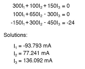
Solving for the Currents
Solving for I1, I2, and I3 using whatever simultaneous equation method we prefer:
Example: Use Octave to find the solution for I1, I2, and I3 from the above-simplified form of equations.
Solution: In Octave, an open-source Matlab® clone, enter the coefficients into the A matrix between square brackets with column elements comma-separated, and rows semicolon-separated. Enter the voltages into the column vector: b. The unknown currents: I1, 2, and I3 are calculated by the command: x=A\b. These are contained within the x column vector.
octave:1>A = [300,100,150;100,650,-300;-150,300,-450]
        A =
          300  100  150
          100  650  -300
          -150 300  -450

        octave:2> b = [0;0;-24]
        b =
          0
          0
          -24

        octave:3> x = A\b
        x =
          -0.093793
           0.077241
           0.136092
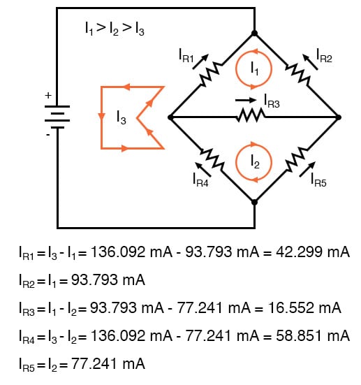
The negative value arrived at for I1 tells us that the assumed direction for that mesh current was incorrect. Thus, the actual current values through each resistor are as such:
Calculating voltage drops across each resistor:
A SPICE simulation confirms the accuracy of our voltage calculations:
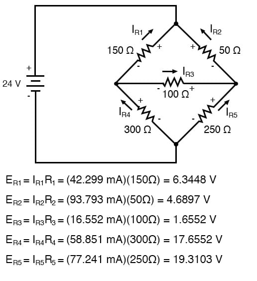
(a) Find a new path for current I3 that does not produce a conflicting polarity on any resistor compared to I1 or I2. R4 was the offending component. (b) Find values for I1, I2, and I3. (c) Find the five resistor currents and compare them to the previous values.
Solution:
(a) Route I3 through R5, R3, and R1 as shown:
Note that the conflicting polarity on R4 has been removed. Moreover, none of the other resistors have conflicting polarities.
(b) Octave, an open source (free) Matlab clone, yields a mesh current vector at “x”:
octave:1> A = [300,100,250;100,650,350;-250,-350,-500]
        A =
          300  100  250
          100  650  350
          -250  -350  -500

        octave:2> b = [0;0;-24]
        b =
          0
          0
        -24

        octave:3> x = A\b
        x =
          -0.093793
          -0.058851
           0.136092
Not all currents I1, I2, and I3 are the same (I2) as the previous bridge because of different loop paths However, the resistor currents compare to the previous values:
        IR1 = I1 + I3 = -93.793 ma + 136.092 ma = 42.299 ma
        IR2 = I1 = -93.793 ma
        IR3 = I1 + I2 + I3 = -93.793 ma -58.851 ma  + 136.092 ma =  -16.552 ma
        IR4 = I2 = -58.851 ma
        IR5 = I2 + I3 = -58.851 ma  + 136.092 ma = 77.241 ma
Since the resistor currents are the same as the previous values, the resistor voltages will be identical and need not be calculated again.
REVIEW:
Steps to follow for the “Mesh Current” method of analysis:
(1) Draw mesh currents in loops of the circuit, enough to account for all components.
(2) Label resistor voltage drop polarities based on assumed directions of mesh currents.
(3) Write KVL equations for each loop of the circuit, substituting the product IR for E in each resistor term of the equation. Where two mesh currents intersect through a component, express the current as of the algebraic sum of those two mesh currents (i.e. I1 + I2) if the currents go in the same direction through that component. If not, express the current as of the difference (i.e. I1 – I2).
(4) Solve for unknown mesh currents (simultaneous equations).
(5) If any solution is negative, then the assumed current direction is wrong!
(6) Algebraically add mesh currents to find current components sharing multiple mesh currents.
(7) Solve for voltage drops across all resistors (E=IR).
Mesh current by inspection
We take a second look at the “mesh current method” with all the currents running clockwise (cw). The motivation is to simplify the writing of mesh equations by ignoring the resistor voltage drop polarity. Though, we must pay attention to the polarity of voltage sources with respect to the assumed current direction. The sign of the resistor voltage drops will follow a fixed pattern.
If we write a set of conventional mesh-current equations for the circuit below, where we do pay attention to the signs of the voltage drop across the resistors, we may rearrange the coefficients into a fixed pattern:
Once rearranged, we may write equations by inspection. The signs of the coefficients follow a fixed pattern in the pair above or the set of three in the rules below.
Mesh current rules:
This method assumes conventional current flow voltage sources. Replace any current source in parallel with a resistor with an equivalent voltage source in series with an equivalent resistance.
Ignoring current direction or voltage polarity on resistors, draw counterclockwise current loops traversing all components. Avoid nested loops.
Write voltage-law equations in terms of unknown currents: I1, I2, and I3. Equation 1 coefficient 1, equation 2, coefficient 2, and equation 3 coefficient 3 are the positive sums of resistors around the respective loops.
All other coefficients are negative, representative of the resistance common to a pair of loops. Equation 1 coefficient 2 is the resistor common to loops 1 and 2, coefficient 3 the resistor common to loops 1 an 3. Repeat for other equations and coefficients.
+(sum of R’s loop 1)I1 – (common R loop 1-2)I2 – (common R loop 1-3)I3 = E1 -(common R loop 1-2)I1 + (sum of R’s loop 2)I2 – (common R loop 2-3)I3 = E2 -(common R loop 1-3)I1 – (common R loop 2-3)I2 + (sum of R’s loop 3)I3 = E3
The right-hand side of the equations is equal to an electron current flow voltage source. A voltage rise with respect to the counterclockwise assumed current is positive, and 0 for no voltage source.
Solve equations for mesh currents: I1, I2, and I3. Solve for currents through individual resistors with KCL. Solve for voltages with Ohms Law and KVL.
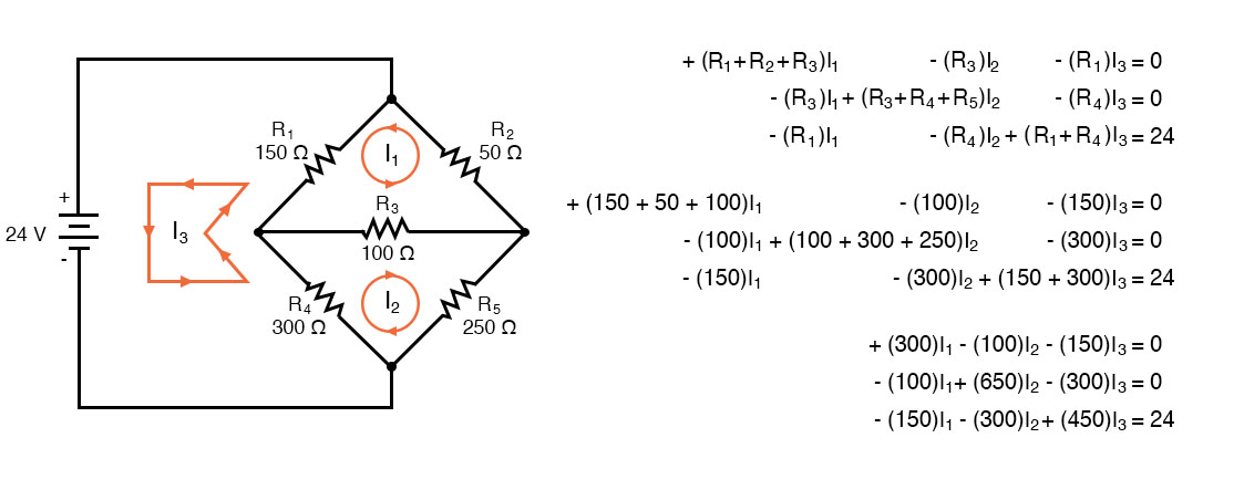
While the above rules are specific for a three mesh circuit, the rules may be extended to smaller or larger meshes. The figure below illustrates the application of the rules. The three currents are all drawn in the same direction, clockwise. One KVL equation is written for each of the three loops. Note that there is no polarity drawn on the resistors. We do not need it to determine the signs of the coefficients. Though we do need to pay attention to the polarity of the voltage source with respect to the current direction. The I3clockwise current flows out from the (+) positive terminal of the l24V source then returns to the (-) terminal. This is a voltage rise for conventional current flow. Therefore, the third equation right-hand side is -24V.
In Octave, enter the coefficients into the A matrix with column elements comma-separated, and rows semicolon-separated. Enter the voltages into the column vector b. Solve for the unknown currents: I1, I2, and I3 with the command: x=A\b. These currents are contained within the x column vector. The positive values indicate that the three mesh currents all flow in the assumed clockwise direction.
octave:2> A=[300,-100,-150;-100,650,-300;-150,-300,450]
           A =
             300  -100  -150
             -100  650  -300
             -150  -300  450

           octave:3> b=[0;0;24]
           b =
              0
              0
             24

           octave:4> x=A\b
           x =
             0.093793
             0.077241
             0.136092
The mesh currents match the previous solution by a different mesh current method. The calculation of resistor voltages and currents will be identical to the previous solution. No need to repeat here.
Note that electrical engineering texts are based on conventional current flow. The loop-current, mesh-current method in those texts will run the assumed mesh currents clockwise. The conventional current flows out the (+) terminal of the battery through the circuit, returning to the (-) terminal. A conventional current-voltage rise corresponds to tracing the assumed current from (-) to (+) through any voltage sources.
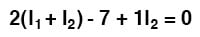
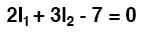
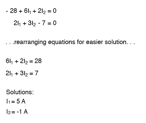
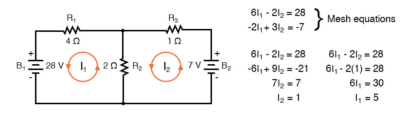
One more example of a previous circuit follows. The resistance around loop 1 is 6 Ω, around loop 2: 3 Ω. The resistance common to both loops is 2 Ω. Note the coefficients of I1 and I2 in the pair of equations. Tracing the assumed clockwise loop 1 current through B1 from (+) to (-) corresponds to an electron current flow voltage rise.
Thus, the sign of the 28 V is positive. The loop 2 counterclockwise assumed current traces (-) to (+) through B2, a voltage drop. Thus, the sign of B2 is negative, -7 in the 2nd mesh equation. Once again, there are no polarity markings on the resistors. Nor do they figure into the equations.
The currents I1 = 5 A, and I2 = 1 A are both positive. They both flow in the direction of the clockwise loops. This compares with previous results.
examples 4.13 and 4.14
Summary:
The modified mesh-current method avoids having to determine the signs of the equation coefficients by drawing all mesh currents clockwise for conventional current flow.
However, we do need to determine the sign of any voltage sources in the loop. The voltage source is positive if the assumed ccw current flows with the battery (source). The sign is negative if the assumed ccw current flows against the battery.