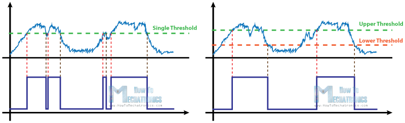
The Schmitt Trigger is a logic input type that provides hysteresis or two different threshold voltage levels for rising and falling edge. This is useful because it can avoid the errors when we have noisy input signals from which we want to get square wave signals.
So for example, if we have a noisy input signal like this, that is meant to have 2 pulses, a device that has only one set point, or threshold, could get incorrect input and it could register more than two pulses as shown in this illustration. And if we use the Schmitt Trigger for the same input signal we will get a correct input of two pulses because of the two different thresholds. So that’s the primal function of the Schmitt Trigger, to convert noisy square waves, sine waves or slow edges inputs into clean square waves.
Types of Schmitt Trigers
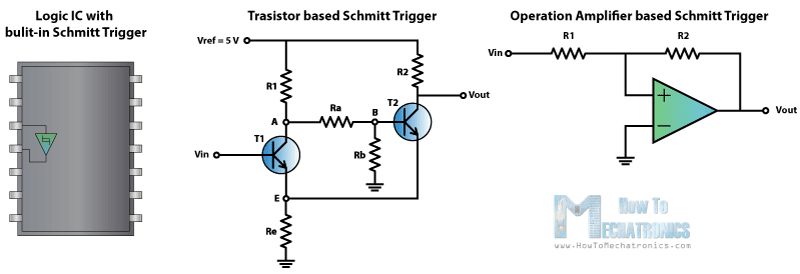
There are many logic ICs that have built-in Schmitt Triggers on their inputs, but also it can be built using transistors or easier using an Operational Amplifier, or comparator and just adding some resistors to it and a positive feedback.
Operational Amplifier based Schmitt Trigger
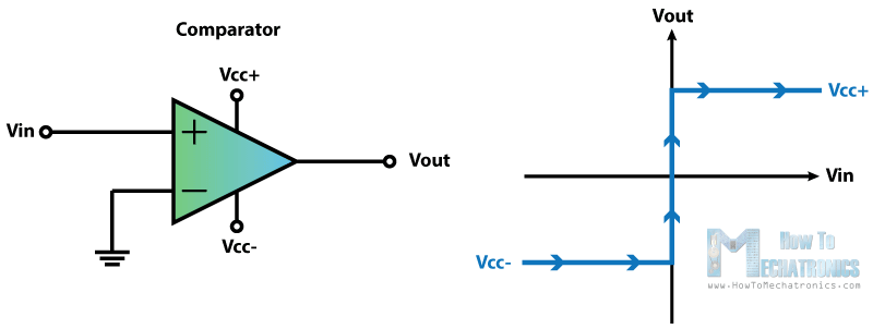
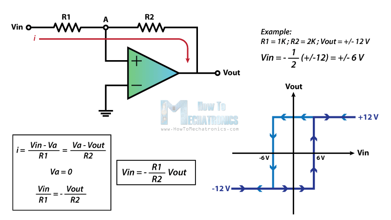
Here we have an op-amp which inverting input is connected to the ground or zero volts and the non-inverting input is connected to a voltage input, VIN. So this is actually a comparator and compares the non-inverting input to the inverting input or in this case the input voltage VIN to 0 V. So when the VIN value is below 0 volts the output of the comparator will be the negative VCC and if the input voltage is above 0 volts the output will be positive VCC.
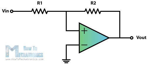
Now if we add a positive feedback by connecting the output voltage to the non-inverting input with a resistor between them and another resistor between the VIN and the non-inverting input we will get the Schmitt Trigger. Now the output will switch from VCC– to VCC+ when the voltage at the A node will cross 0 volts.
That means that now by adjusting the values of the resistors we can set at what value of the VIN input the switch will occur using the following equations. We get these equations with the following relationships. The current “i” through this line equals VIN – VA divided by R1 as well as VA – VOUT divided by R2. So if we replace the VA with zero, as we need that value for the switch to occur, we will get that final equation. For example if the output is -12 volts and the VIN input is negative and rises, the switch from -12 V to +12 V will occur at 6 volts according to the equation and the values of the resistors and vice versa when the VIN input is high and declines the switch from +12 V to – 12V will occur at -6 volts.
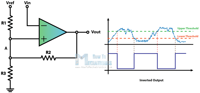
Non-Symmetrical Schmitt Trigger
In order to get two different non-symmetrical thresholds, we can use this circuit of an inverting single powered Schmitt Trigger. Here the VREF voltage is the same as the VCC of the op-amp. Now because the VIN input is connected to the inverting input of the op-amp when its values will reach the upper threshold, the output will switch off to 0 volts, and then when its values will decline to the lower threshold, the output will switch on to 5 volts.
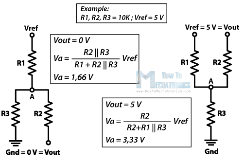
Here’s an example of how we can calculate the thresholds. The VREF and the VCC will be 5 volts and the three resistors will be the same 10k ohms. So what we need to calculate now is the voltage at the A node. In the first case when the output is 0 V our circuit will look like this, a simple voltage divider and the value of the VA will be 1.66 V. This means that the VIN input needs to decline below that value in order the output to switch on to 5 volts. Now with this 5 volts at the output the circuit will look like this. The value of the VA will be 3.33 V. This means that the VIN input needs to rise above that value in order the output to switch off to 0 volts.
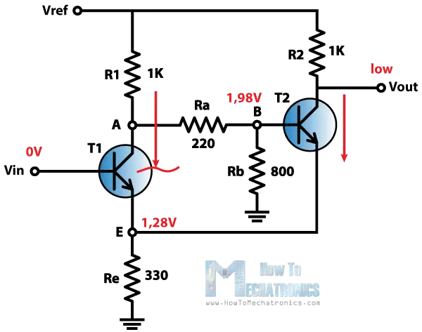
The Schmitt Trigger is a logic input type that provides hysteresis or two different threshold voltage levels for rising and falling edge. This is useful because it can avoid the errors when we have noisy input signals from which we want to get square wave signals. The Transistor Schmitt Triger circuit contains two transistors and five resistors. For better explanation I will assign values to the components, and later I will make demonstration and build this circuit on a protoboard to see how it really works.
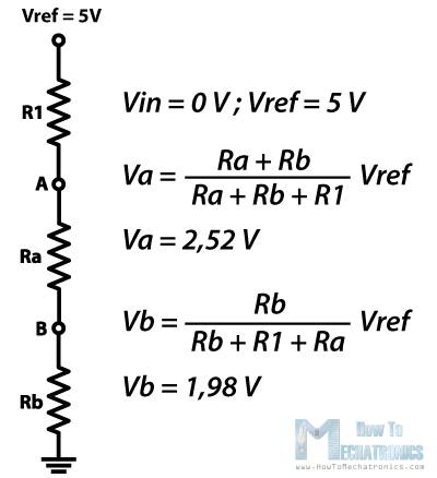
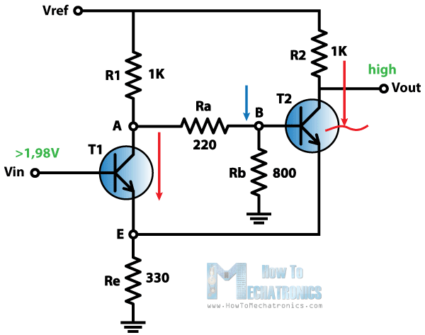
We will start like this. Let’s suppose that the Vin input is 0 V. That means that transistor T1 is cut off and not conducting. On the other hand the Transistor T2 is conducting because we have a voltage of about 1.98 V at the B node as we can consider this part of the circuit as a voltage divider and calculate the voltage using this expressions.
So because the Transistor T2 is conducting the output voltage will be low and the voltage at the emitter will be about 0.7 V lower than the voltage at the base of the transistor, or that’s about 1.28 V.
The emitter of the transistor T1 is connected with the emitter of the transistor T2 so they are at the same voltage level of 1.28 V which means that the transistor T1 will turn on when the voltage Vin at its base will be 0.7 V above this value of 1.28 V, or about 1.98 V.
So as we increase the Vin input and we cross this value of 1.98 the transistor T1 will start conducting. This will cause the voltage at the base of the transistor T2 to drop and will cut the transistor off. As the transistor T2 is no longer conducting the output voltage will go high.
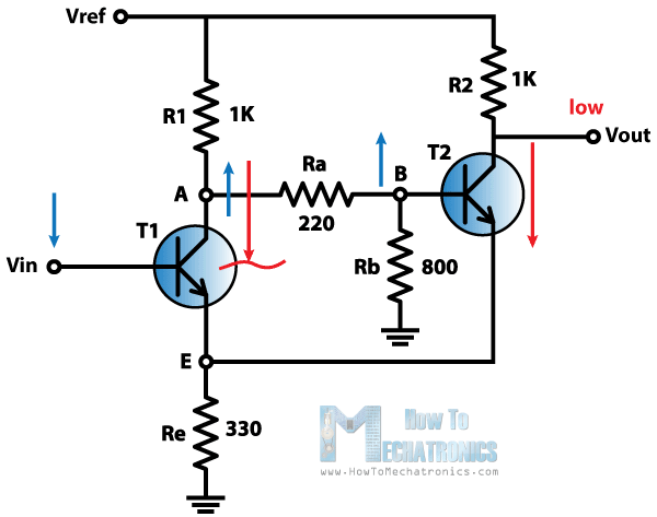
Next, the voltage Vin at the base of the transistor T1 will start declining and it will turn the transistor off when the base voltage will be 0.7 V above the voltage of its emitter. This will happen as the current in the emitter will decline to a point where the transistor will get into forward-active mode. In this mode the collector voltage will increase, which will also increase the voltage at the base of the transistor T2. This will cause small amount of current to flow through the transistor T2 which will further drop the voltage at the emitters and will cause the transistor T1 to turn off. In our case the Vin input needs to drop to about 1.3 V to turn off the transistor T1.
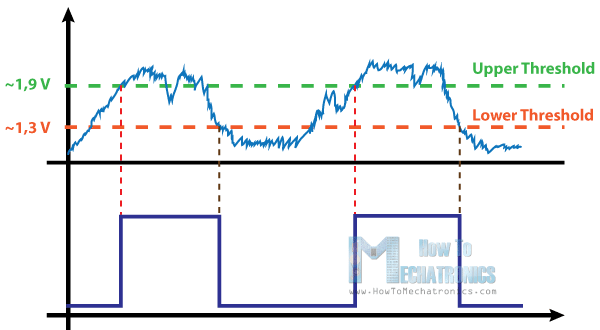
That’s it. Now the cycle repeats over and over again. So we got two thresholds, the high threshold at about 1.9 V and the low threshold at about 1.3 V.
we can volt at node A by use thevenin’s theorem if vref =5 and vin=1.4 and hfe=220
note: in the previous circuit the current pass the transistor is constant current not affected by remaining of the circuit because that we not use the emitter resistor to calculate Rth
current limiter circuit Rcl between BJT base and its emitter increase the current flow of regulator by add transisotr foldback to protect circuit from over current isc = current in short circuit imax=max current can flowvoltage regulator + current limitermore flow current not recommended to use left top schematic because some transistors have hfe and voltage drop more than another one from same mode that mean it can flow more current so its heated faster and pass more current(thermal runaway) so you prefer to add resistor at emitter to keep all transistors passes current evenly and you can add limiter to protect itparallel mosfets for share current only work with switch mode (cutoff or saturation)at active linear region you should to add resistor after source … and you can add transistor and resistor for current limiter ….lm317 schematic it is too similar to figure 3 … and over temp and over current protection is actually like current limiter and foldback blocksconstant current load
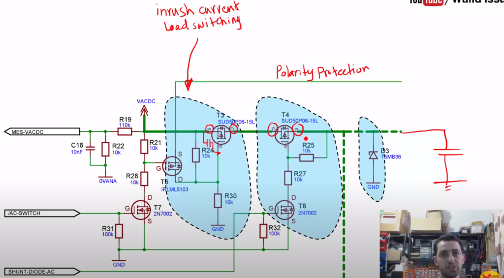
inrush current protector to protect capacitor from fast charging and let mosfets work as soft start + polarity protection in the same schematic
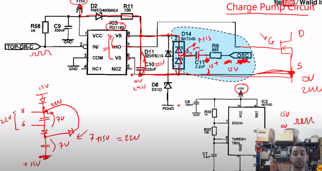
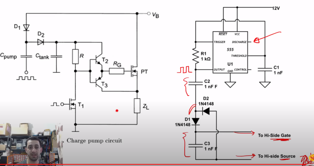
charge pump circuit or bootstrap (diodes + capacitors+ pwm signal)
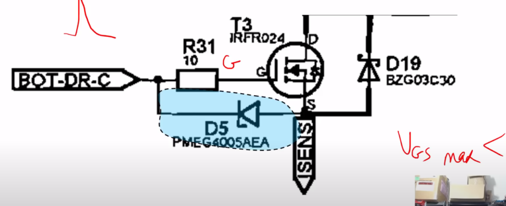
gate voltage protection
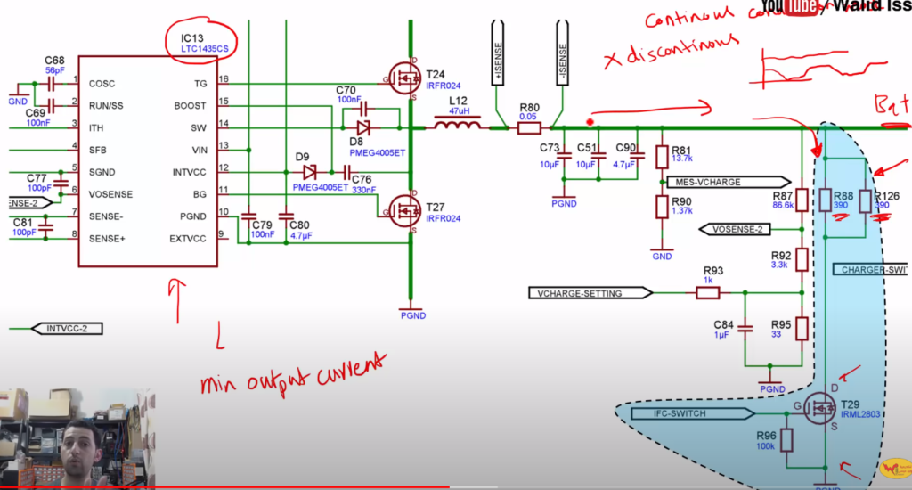
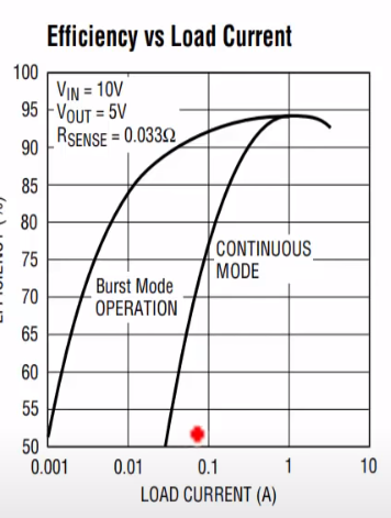
some ics need minimum output current or continious conduction mode
used with ic if it work with minimum output current or work with continious conduction modediscontiniuos conduction mode mod some ic struggling with it so you should to put ic in continous mode
multi sources diodes
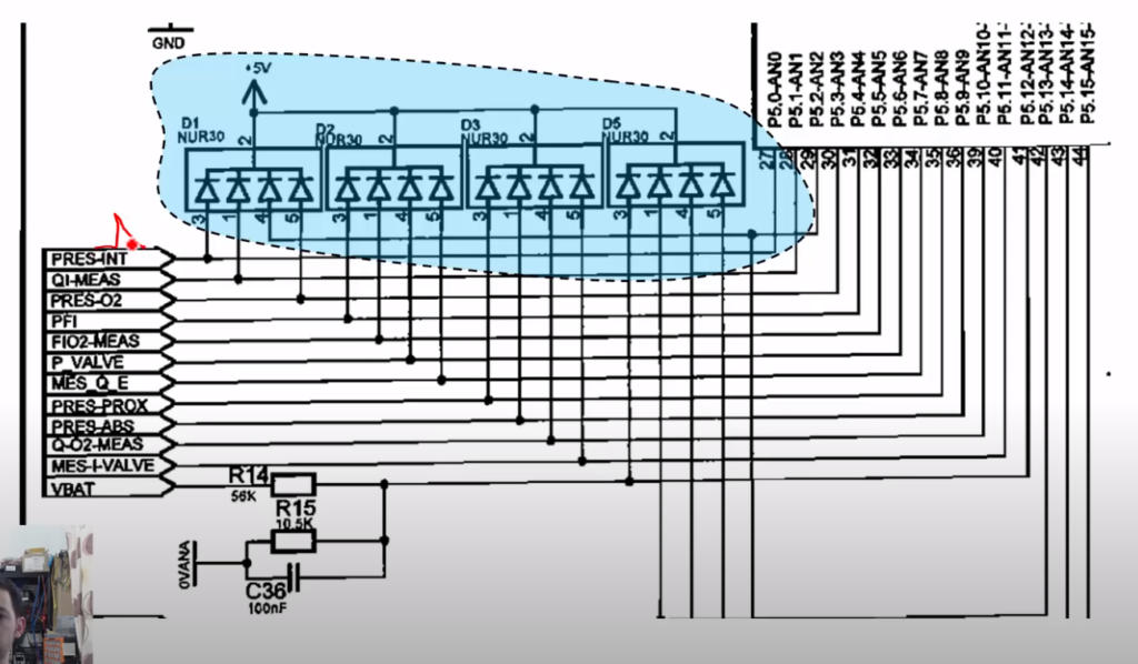
hystarisis comparator
put capacitors with voltage divider
voltage regulator ic vs voltage reference ic
before any ic source we put capacitors for decobling and some times we need more than one parallel capacitor for lower esr and more smoothing
The most common amplifier configuration for an NPN transistor is that of the Common Emitter Amplifier circuit
All types of transistor amplifiers operate using AC signal inputs which alternate between a positive value and a negative value so some way of “presetting” the amplifier circuit to operate between these two maximum or peak values is required. This is achieved using a process known as Biasing. Biasing is very important in amplifier design as it establishes the correct operating point of the transistor amplifier ready to receive signals, thereby reducing any distortion to the output signal.
We also saw that a static or DC load line can be drawn onto these output characteristics curves to show all the possible operating points of the transistor from fully “ON” to fully “OFF”, and to which the quiescent operating point or Q-point of the amplifier can be found.
The aim of any small signal amplifier is to amplify all of the input signal with the minimum amount of distortion possible to the output signal, in other words, the output signal must be an exact reproduction of the input signal but only bigger (amplified).
To obtain low distortion when used as an amplifier the operating quiescent point needs to be correctly selected. This is in fact the DC operating point of the amplifier and its position may be established at any point along the load line by a suitable biasing arrangement.
The best possible position for this Q-point is as close to the center position of the load line as reasonably possible, thereby producing a Class A type amplifier operation, ie. Vce = 1/2Vcc. Consider the Common Emitter Amplifier circuit shown below.
The Common Emitter Amplifier Circuit
The single stage common emitter amplifier circuit shown above uses what is commonly called “Voltage Divider Biasing”. This type of biasing arrangement uses two resistors as a potential divider network across the supply with their center point supplying the required Base bias voltage to the transistor. Voltage divider biasing is commonly used in the design of bipolar transistor amplifier circuits.
This method of biasing the transistor greatly reduces the effects of varying Beta, ( β ) by holding the Base bias at a constant steady voltage level allowing for best stability. The quiescent Base voltage (Vb) is determined by the potential divider network formed by the two resistors, R1, R2 and the power supply voltage Vcc as shown with the current flowing through both resistors.
Then the total resistance RT will be equal to R1 + R2 giving the current as i = Vcc/RT. The voltage level generated at the junction of resistors R1 and R2 holds the Base voltage (Vb) constant at a value below the supply voltage.
Then the potential divider network used in the common emitter amplifier circuit divides the supply voltage in proportion to the resistance. This bias reference voltage can be easily calculated using the simple voltage divider formula below:
Transistor Bias Voltage
The same supply voltage, (Vcc) also determines the maximum Collector current, Ic when the transistor is switched fully “ON” (saturation), Vce = 0. The Base current Ib for the transistor is found from the Collector current, Ic and the DC current gain Beta, β of the transistor.
Beta Value
Beta is sometimes referred to as hFE which is the transistors forward current gain in the common emitter configuration. Beta has no units as it is a fixed ratio of the two currents, Ic and Ib so a small change in the Base current will cause a large change in the Collector current.
One final point about Beta. Transistors of the same type and part number will have large variations in their Beta value. For example, the BC107 NPN Bipolar transistor has a DC current gain Beta value of between 110 and 450 (data sheet value). So one BC107 may have a Beta value of 110, while another one may have a Beta value of 450, but they are both BC107 npn transistors. This is because Beta is a characteristic of the transistors construction and not of its operation.
As the Base/Emitter junction is forward-biased, the Emitter voltage, Ve will be one junction voltage drop different to the Base voltage. If the voltage across the Emitter resistor is known then the Emitter current, Ie can be easily calculated using Ohm’s Law. The Collector current, Ic can be approximated, since it is almost the same value as the Emitter current.
Common Emitter Amplifier Example No1
An common emitter amplifier circuit has a load resistance, RL of 1.2kΩ and a supply voltage of 12v. Calculate the maximum Collector current (Ic) flowing through the load resistor when the transistor is switched fully “ON” (saturation), assume Vce = 0. Also find the value of the Emitter resistor, RE if it has a voltage drop of 1v across it. Calculate the values of all the other circuit resistors assuming a standard NPN silicon transistor.
This then establishes point “A” on the Collector current vertical axis of the characteristics curves and occurs when Vce = 0. When the transistor is switched fully “OFF”, their is no voltage drop across either resistor RE or RL as no current is flowing through them. Then the voltage drop across the transistor, Vce is equal to the supply voltage, Vcc. This establishes point “B” on the horizontal axis of the characteristics curves.
Generally, the quiescent Q-point of the amplifier is with zero input signal applied to the Base, so the Collector sits about half-way along the load line between zero volts and the supply voltage, (Vcc/2). Therefore, the Collector current at the Q-point of the amplifier will be given as:
This static DC load line produces a straight line equation whose slope is given as: -1/(RL + RE) and that it crosses the vertical Ic axis at a point equal to Vcc/(RL + RE). The actual position of the Q-point on the DC load line is determined by the mean value of Ib.
As the Collector current, Ic of the transistor is also equal to the DC gain of the transistor (Beta), times the Base current (β*Ib), if we assume a Beta (β) value for the transistor of say 100, (one hundred is a reasonable average value for low power signal transistors) the Base current Ib flowing into the transistor will be given as:
Instead of using a separate Base bias supply, it is usual to provide the Base Bias Voltage from the main supply rail (Vcc) through a dropping resistor, R1. Resistors, R1 and R2 can now be chosen to give a suitable quiescent Base current of 45.8μA or 46μA rounded off to the nearest integer. The current flowing through the potential divider circuit has to be large compared to the actual Base current, Ib, so that the voltage divider network is not loaded by the Base current flow.
A general rule of thumb is a value of at least 10 times Ib flowing through the resistor R2. Transistor Base/Emitter voltage, Vbe is fixed at 0.7V (silicon transistor) then this gives the value of R2 as:
If the current flowing through resistor R2 is 10 times the value of the Base current, then the current flowing through resistor R1 in the divider network must be 11 times the value of the Base current. That is: IR2 + Ib.
Thus the voltage across resistor R1 is equal to Vcc – 1.7v (VRE + 0.7 for silicon transistor) which is equal to 10.3V, therefore R1 can be calculated as:
The value of the Emitter resistor, RE can be easily calculated using Ohm’s Law. The current flowing through RE is a combination of the Base current, Ib and the Collector current Ic and is given as:
Resistor, RE is connected between the transistors Emitter terminal and ground, and we said previously that there is a voltage drop of 1 volt across it. Thus the value of the Emitter resistor, RE is calculated as:
So, for our example above, the preferred values of the resistors chosen to give a tolerance of 5% (E24) are:
Then, our original Common Emitter Amplifier circuit above can be rewritten to include the values of the components that we have just calculated above.
Completed Common Emitter Circuit
Amplifier Coupling Capacitors
In Common Emitter Amplifier circuits, capacitors C1 and C2 are used as Coupling Capacitors to separate the AC signals from the DC biasing voltage. This ensures that the bias condition set up for the circuit to operate correctly is not affected by any additional amplifier stages, as the capacitors will only pass AC signals and block any DC component. The output AC signal is then superimposed on the biasing of the following stages. Also a bypass capacitor, CE is included in the Emitter leg circuit.
This capacitor is effectively an open circuit component for DC biasing conditions, which means that the biasing currents and voltages are not affected by the addition of the capacitor maintaining a good Q-point stability.
However, this parallel connected bypass capacitor effectively becomes a short circuit to the Emitter resistor at high frequency signals due to its reactance. Thus only RL plus a very small internal resistance acts as the transistors load increasing voltage gain to its maximum. Generally, the value of the bypass capacitor, CE is chosen to provide a reactance of at most, 1/10th the value of RE at the lowest operating signal frequency.
Output Characteristics Curves
Ok, so far so good. We can now construct a series of curves that show the Collector current, Ic against the Collector/Emitter voltage, Vce with different values of Base current, Ib for our simple common emitter amplifier circuit.
These curves are known as the “Output Characteristic Curves” and are used to show how the transistor will operate over its dynamic range. A static or DC load line is drawn onto the curves for the load resistor RL of 1.2kΩ to show all the transistors possible operating points.
When the transistor is switched “OFF”, Vce equals the supply voltage Vcc and this is point “B” on the line. Likewise when the transistor is fully “ON” and saturated the Collector current is determined by the load resistor, RL and this is point “A” on the line.
We calculated before from the DC gain of the transistor that the Base current required for the mean position of the transistor was 45.8μA and this is marked as point Q on the load line which represents the Quiescent point or Q-point of the amplifier. We could quite easily make life easy for ourselves and round off this value to 50μA exactly, without any effect to the operating point.
Output Characteristics Curves
Point Q on the load line gives us the Base current Q-point of Ib = 45.8μA or 46μA. We need to find the maximum and minimum peak swings of Base current that will result in a proportional change to the Collector current, Ic without any distortion to the output signal.
As the load line cuts through the different Base current values on the DC characteristics curves we can find the peak swings of Base current that are equally spaced along the load line. These values are marked as points “N” and “M” on the line, giving a minimum and a maximum Base current of 20μA and 80μA respectively.
These points, “N” and “M” can be anywhere along the load line that we choose as long as they are equally spaced from Q. This then gives us a theoretical maximum input signal to the Base terminal of 60μA peak-to-peak, (30μA peak) without producing any distortion to the output signal.
Any input signal giving a Base current greater than this value will drive the transistor to go beyond point “N” and into its “cut-off” region or beyond point “M” and into its Saturation region thereby resulting in distortion to the output signal in the form of “clipping”.
Using points “N” and “M” as an example, the instantaneous values of Collector current and corresponding values of Collector-emitter voltage can be projected from the load line. It can be seen that the Collector-emitter voltage is in anti-phase (–180o) with the collector current.
As the Base current Ib changes in a positive direction from 50μA to 80μA, the Collector-emitter voltage, which is also the output voltage decreases from its steady state value of 5.8 volts to 2.0 volts.
Then a single stage Common Emitter Amplifier is also an “Inverting Amplifier” as an increase in Base voltage causes a decrease in Vout and a decrease in Base voltage produces an increase in Vout. In other words the output signal is 180o out-of-phase with the input signal.
Common Emitter Voltage Gain
The Voltage Gain of the common emitter amplifier is equal to the ratio of the change in the input voltage to the change in the amplifiers output voltage. Then ΔVL is Vout and ΔVB is Vin. But voltage gain is also equal to the ratio of the signal resistance in the Collector to the signal resistance in the Emitter and is given as:
We mentioned earlier that as the signal frequency increases the bypass capacitor, CE starts to short out the Emitter resistor due to its reactance. Then at high frequencies RE = 0, making the gain infinite.
However, bipolar transistors have a small internal resistance built into their Emitter region called Re. The transistors semiconductor material offers an internal resistance to the flow of current through it and is generally represented by a small resistor symbol shown inside the main transistor symbol.
Transistor data sheets tell us that for a small signal bipolar transistors this internal resistance is the product of 25mV ÷ Ie (25mV being the internal volt drop across the Emitter junction layer), then for our common Emitter amplifier circuit above this resistance value will be equal to:
This internal Emitter leg resistance will be in series with the external Emitter resistor, RE, then the equation for the transistors actual gain will be modified to include this internal resistance so will be:
At low frequency signals the total resistance in the Emitter leg is equal to RE + Re. At high frequency, the bypass capacitor shorts out the Emitter resistor leaving only the internal resistance Re in the Emitter leg resulting in a high gain. Then for our common emitter amplifier circuit above, the gain of the circuit at both low and high signal frequencies is given as:
Gain at Low Frequencies
Gain at High Frequencies
One final point, the voltage gain is dependent only on the values of the Collector resistor, RL and the Emitter resistance, (RE + Re) it is not affected by the current gain Beta, β (hFE) of the transistor.
So, for our simple example above we can now summarise all the values we have calculated for our common emitter amplifier circuit and these are:
Minimum
Mean
Maximum
Base Current
20μA
50μA
80μA
Collector Current
2.0mA
4.8mA
7.7mA
Output Voltage Swing
2.0V
5.8V
9.3V
Amplifier Gain
-5.32
-218
Common Emitter Amplifier Summary
Then to summarise. The Common Emitter Amplifier circuit has a resistor in its Collector circuit. The current flowing through this resistor produces the voltage output of the amplifier. The value of this resistor is chosen so that at the amplifiers quiescent operating point, Q-point this output voltage lies half way along the transistors load line.
The Base of the transistor used in a common emitter amplifier is biased using two resistors as a potential divider network. This type of biasing arrangement is commonly used in the design of bipolar transistor amplifier circuits and greatly reduces the effects of varying Beta, ( β ) by holding the Base bias at a constant steady voltage. This type of biasing produces the greatest stability.
A resistor can be included in the emitter leg in which case the voltage gain becomes -RL/RE. If there is no external Emitter resistance, the voltage gain of the amplifier is not infinite as there is a very small internal resistance, Re in the Emitter leg. The value of this internal resistance is equal to 25mV/IE