Transistor Capacitance Multiplier

The basic capacitance multiplier circuit is essentially a simple emitter follower with a capacitor on the base and a feed resistor from the input to the base to turn the transistor on. A capacitor from the base to ground provides the smoothing.

Basic transistor capacitance multiplier circuit
Basic transistor capacitance multiplier

The capacitance multiplier circuit operation is quite straightforward. It acts as a simple emitter follower. The resistor R1 provides bias for the base emitter junction, and the capacitor provides smoothing. This considerably reduces the levels on noise on the output, i.e. Vout.

The effect of placing the transistor in the circuit is that it effectively multiplies the capacitance on the base by the current gain of the transistor, i.e. by β

The capacitance multiplier circuit is not a voltage regulator. The output voltage varies directly with the input Vin as there is no voltage reference. Generally the output voltage is about 0.65V less than the base voltage, and around 2 – 3 V less than Vin when a load is applied.

The ripple and noise levels on the output can be reduced to very low levels> Increasing the values of R1 and C1 reduce the output ripple, and increasingly at low frequencies. On the downside large values of R1 and C1 cause the output to rise slowly towards the required value after turn on, because of the large time constant of R1 and C1.

Modified capacitance multiplier

The drawback of the circuit is that in its basic form, there is very little voltage drop across the series pass transistor, and noise reduction is not as high as it may be. To overcome this, some people place a resistor across the capacitor and this provides a potential divider reducing the voltage at the base and increasing the voltage drop across the transistor. This enables it to provide better noise reduction, although it does increase power dissipation and reduces the voltage at Vout.

Basic transistor capacitance multiplier circuit incorporating a bias potential divider
Basic transistor capacitance multiplier with a potential divider

This version of the capacitance multiplier circuit includes an additional resistor from the base to ground to reduce the base voltage and provide additional voltage drop across the transistor for improved smoothing. This is more important when the levels of ripple are higher.

Typically the voltage through the potential divider should be sufficient to maintain the base voltage sufficiently. A judgement can be made regarding the level of current though the potential divider, but often in these types of circuits it may be ten times the base current. This would ensure that the emitter voltage is maintained over a wide range of output current levels.

Example application for a capacitance multiplier

The power supply shown here provides only smoothing at this stage and no stabilisation or voltage regulation. The input is taken from the mains and rectified by the bridge rectifier. It then passes into a smoothing capacitor, C1, to provide the first smoothing and remove the major ripple. This capacitor should have a large ripple current capability if the supply is to be used for high current levels.

It should be remembered that the capacitance multiplication effect can only be realised if there is a sufficient voltage drop across the series transistor. Typically this should be a minimum of 3 volts at all times.

The capacitor C2 is connected to the base of the transistor TR1. This provides the capacitance for the capacitance multiplication effect.

TR1 is the main pass transistor and must be able to drop the required voltage and at the required current, so power dissipation may need to be calculated.

Example application for a capacitance multiplier

On the output there is a capacitor to provide a little further decoupling and to ensure that the circuit remains stable. The resistor ensures the output voltage drains away at power removal. The diode D1 ensures that the transistor does not become reverse biased.

Unusual Transistors Circuits

Diod Transistors

Transistor as a Zener

Zener diodes connected as shown in Fig. 1 are carefully doped at manufacture such that they break down when a critical reverse bias voltage is applied and allows current to flow. The current is limited by the power ratings of the particular device employed.

Zeners are used to provide a voltage reference and any transistor can be employed to do the same job if connected as shown in Fig. 2.

Different transistors will produce different zener voltages and a series of tests can be done to establish what the typical zener voltage is for that device.

A suitable setup could be employed as shown below.

  A BC548B gives a zener voltage Vz = 8.2V

  A BC549B gives a zener voltage Vz = 10.8V

  A BC547B gives a zener voltage Vz = 9.1V

  A BC184 gives a zener voltage Vz = 8.2V

Using the Configuration in Practice

The above circuit Fig 4 could form the basis of a low power regulated power supply.

Vbe Multiplayer

Variable Reference Voltage Circuit

Fig. 5 shows a way of adjusting the voltage Vz to suit by adjusting the resistor values of R1 and R2.

Vz = Vbe((R1 + R2)/R2)

Better regulation can be achieved with a darlington configuration as shown below where it is used in a simple regulated supply, but now the voltage Vz becomes:-

Vz = 2Vbe((R1 + R2)/R2)

and the regulated output voltage becomes:-

Vo = Vz – Vbe

Other more circuits

any signal add to it vbe by Q1 and send it to Q2 so Q2 can read any signal
vce more stable than vbe because once vbe increased R2 incresed and keep palance
Vbe multiplayer with more stability

Why Parallel Capacitors?

Calculating ripple voltage and current

To choose the right capacitor for the input filter of a switching regulator, for example, the capacitance needed to achieve a desired voltage ripple can be calculated, if the operating conditions of the regulator are known. When the capacitance is calculated, a candidate component can be identified, and the ripple current determined from the known ESR. This ripple current must be within the capacitor’s ripple current handling capability, if the device is to be suitable for use. This is where selection can become difficult, because both ESR and capacitance are known to vary with temperature, operating frequency, and the applied DC bias.

The capacitance can be calculated using the equation (from TI Application Report SLTA055)

Where CMIN = minimum capacitance required

IOUT = output current

dc = duty cycle (usually calculated as dc=Vout/(Vin*Eff))

fSW = switching frequency

VP(max) = peak-to-peak ripple voltage

Assuming, for example, a regulator with 12v input; 5v output; 2amp output; 85% efficiency; 400kHz switching, and an allowable input ripple voltage of 65mV:

Note that the chosen device must provide this value of capacitance at the regulator operating frequency of 400kHz.

The rms value of the peak-to-peak ripple voltage can be calculated from the equation:

Vrms=Vpp*1/(2*√2)

The ripple current in the capacitor can then be calculated by applying Ohm’s law, if the capacitor’s ESR is known.

Op-amp Circuits

Inverting

Amplifiers or any operational amplifier for that matter and these are.

  • No Current Flows into the Input Terminals
  • The Differential Input Voltage is Zero as V1 = V2 = 0 (Virtual Earth)

Then by using these two rules we can derive the equation for calculating the closed-loop gain of an inverting amplifier, using first principles.

Current ( i ) flows through the resistor network as shown.

resistor feedback circuit
inverting op-amp gain formula

Then, the Closed-Loop Voltage Gain of an Inverting Amplifier is given as.

inverting operational amplifier gain equation

and this can be transposed to give Vout as:

inverting operational amplifier gain

Non-inverting

non-inverting operational amplifier

In the previous Inverting Amplifier tutorial, we said that for an ideal op-amp “No current flows into the input terminal” of the amplifier and that “V1 always equals V2”. This was because the junction of the input and feedback signal ( V1 ) are at the same potential.

In other words the junction is a “virtual earth” summing point. Because of this virtual earth node the resistors, Rƒ and R2 form a simple potential divider network across the non-inverting amplifier with the voltage gain of the circuit being determined by the ratios of R2 and Rƒ as shown below.

Equivalent Potential Divider Network

non-inverting amplifier potential divider

Then using the formula to calculate the output voltage of a potential divider network, we can calculate the closed-loop voltage gain ( AV ) of the Non-inverting Amplifier as follows:

non-inverting op-amp gain

Then the closed loop voltage gain of a Non-inverting Operational Amplifier will be given as:

non-inverting operational amplifier gain

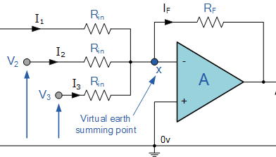
Summing

summing amplifier

In this simple summing amplifier circuit, the output voltage, ( Vout ) now becomes proportional to the sum of the input voltages, V1, V2, V3, etc. Then we can modify the original equation for the inverting amplifier to take account of these new inputs thus:

summing amplifier formula

However, if all the input impedances, ( RIN ) are equal in value, we can simplify the above equation to give an output voltage of:

Summing Amplifier Equation

summing amplifier equation

Differential Amplifier

differential amplifier circuit

By connecting each input in turn to 0v ground we can use superposition to solve for the output voltage Vout. Then the transfer function for a Differential Amplifier circuit is given as:

differential amplifier transfer function

When resistors, R1 = R2 and R3 = R4 the above transfer function for the differential amplifier can be simplified to the following expression:

Differential Amplifier Equation

differential amplifier equation

Op-amp Integrator Circuit

op-amp integrator amplifier circuit
op-amp integrator equation

To simplify the math’s a little, this can also be re-written as:

simplified integrator equation

notes:
if Vin is constant voltage so Rin voltage drop always equal Vin so it is feeding C with constant current source for example if we have capacitor with 1H and constant current source 1A every seconds the capacitor it will increase 1 volt constantly Vin/(Rin.C)

Op-amp Differentiator Circuit

op-amp differential amplifier
op-amp differentiator equation