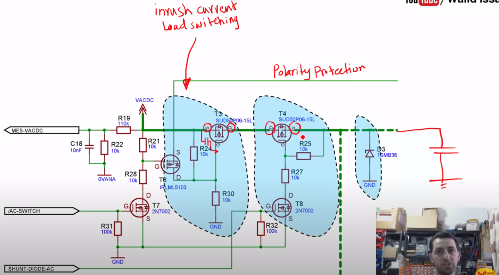
inrush current protector to protect capacitor from fast charging and let mosfets work as soft start + polarity protection in the same schematic
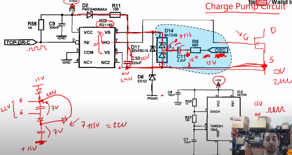
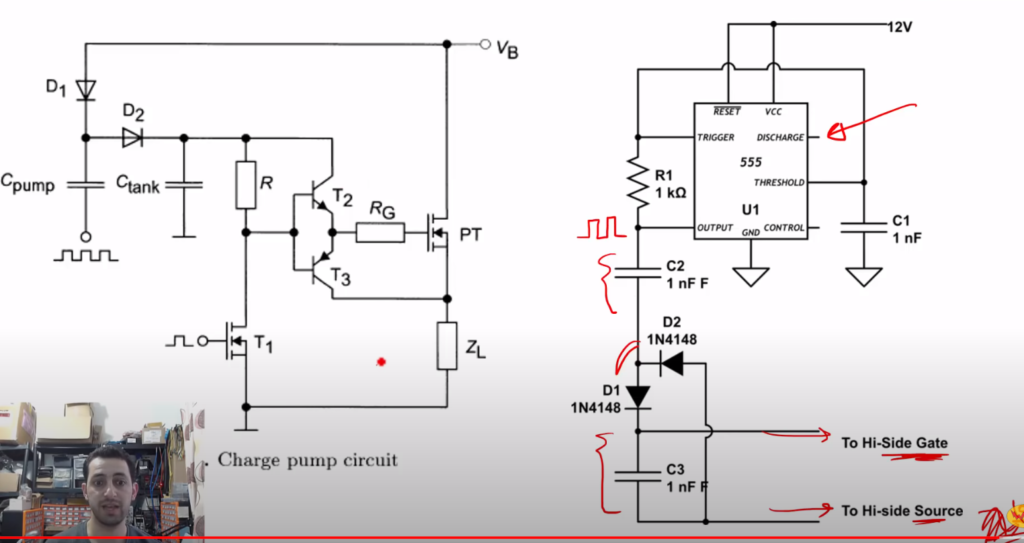
charge pump circuit or bootstrap (diodes + capacitors+ pwm signal)
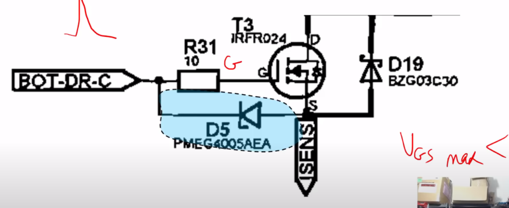
gate voltage protection
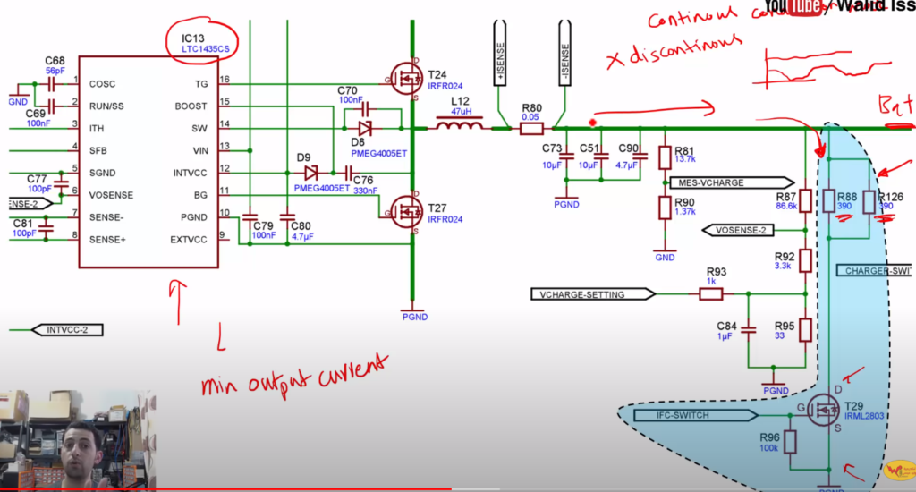
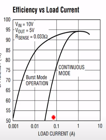
some ics need minimum output current or continious conduction mode
used with ic if it work with minimum output current or work with continious conduction modediscontiniuos conduction mode mod some ic struggling with it so you should to put ic in continous mode
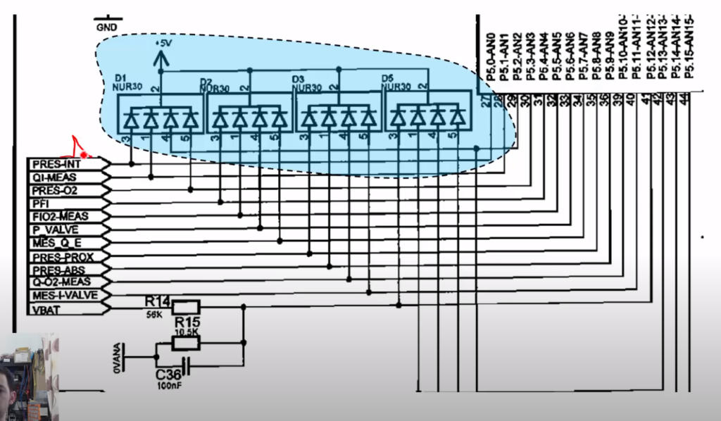
multi sources diodes
hystarisis comparator
put capacitors with voltage divider
voltage regulator ic vs voltage reference ic
before any ic source we put capacitors for decobling and some times we need more than one parallel capacitor for lower esr and more smoothing
The most common amplifier configuration for an NPN transistor is that of the Common Emitter Amplifier circuit
All types of transistor amplifiers operate using AC signal inputs which alternate between a positive value and a negative value so some way of “presetting” the amplifier circuit to operate between these two maximum or peak values is required. This is achieved using a process known as Biasing. Biasing is very important in amplifier design as it establishes the correct operating point of the transistor amplifier ready to receive signals, thereby reducing any distortion to the output signal.
We also saw that a static or DC load line can be drawn onto these output characteristics curves to show all the possible operating points of the transistor from fully “ON” to fully “OFF”, and to which the quiescent operating point or Q-point of the amplifier can be found.
The aim of any small signal amplifier is to amplify all of the input signal with the minimum amount of distortion possible to the output signal, in other words, the output signal must be an exact reproduction of the input signal but only bigger (amplified).
To obtain low distortion when used as an amplifier the operating quiescent point needs to be correctly selected. This is in fact the DC operating point of the amplifier and its position may be established at any point along the load line by a suitable biasing arrangement.
The best possible position for this Q-point is as close to the center position of the load line as reasonably possible, thereby producing a Class A type amplifier operation, ie. Vce = 1/2Vcc. Consider the Common Emitter Amplifier circuit shown below.
The Common Emitter Amplifier Circuit
The single stage common emitter amplifier circuit shown above uses what is commonly called “Voltage Divider Biasing”. This type of biasing arrangement uses two resistors as a potential divider network across the supply with their center point supplying the required Base bias voltage to the transistor. Voltage divider biasing is commonly used in the design of bipolar transistor amplifier circuits.
This method of biasing the transistor greatly reduces the effects of varying Beta, ( β ) by holding the Base bias at a constant steady voltage level allowing for best stability. The quiescent Base voltage (Vb) is determined by the potential divider network formed by the two resistors, R1, R2 and the power supply voltage Vcc as shown with the current flowing through both resistors.
Then the total resistance RT will be equal to R1 + R2 giving the current as i = Vcc/RT. The voltage level generated at the junction of resistors R1 and R2 holds the Base voltage (Vb) constant at a value below the supply voltage.
Then the potential divider network used in the common emitter amplifier circuit divides the supply voltage in proportion to the resistance. This bias reference voltage can be easily calculated using the simple voltage divider formula below:
Transistor Bias Voltage
The same supply voltage, (Vcc) also determines the maximum Collector current, Ic when the transistor is switched fully “ON” (saturation), Vce = 0. The Base current Ib for the transistor is found from the Collector current, Ic and the DC current gain Beta, β of the transistor.
Beta Value
Beta is sometimes referred to as hFE which is the transistors forward current gain in the common emitter configuration. Beta has no units as it is a fixed ratio of the two currents, Ic and Ib so a small change in the Base current will cause a large change in the Collector current.
One final point about Beta. Transistors of the same type and part number will have large variations in their Beta value. For example, the BC107 NPN Bipolar transistor has a DC current gain Beta value of between 110 and 450 (data sheet value). So one BC107 may have a Beta value of 110, while another one may have a Beta value of 450, but they are both BC107 npn transistors. This is because Beta is a characteristic of the transistors construction and not of its operation.
As the Base/Emitter junction is forward-biased, the Emitter voltage, Ve will be one junction voltage drop different to the Base voltage. If the voltage across the Emitter resistor is known then the Emitter current, Ie can be easily calculated using Ohm’s Law. The Collector current, Ic can be approximated, since it is almost the same value as the Emitter current.
Common Emitter Amplifier Example No1
An common emitter amplifier circuit has a load resistance, RL of 1.2kΩ and a supply voltage of 12v. Calculate the maximum Collector current (Ic) flowing through the load resistor when the transistor is switched fully “ON” (saturation), assume Vce = 0. Also find the value of the Emitter resistor, RE if it has a voltage drop of 1v across it. Calculate the values of all the other circuit resistors assuming a standard NPN silicon transistor.
This then establishes point “A” on the Collector current vertical axis of the characteristics curves and occurs when Vce = 0. When the transistor is switched fully “OFF”, their is no voltage drop across either resistor RE or RL as no current is flowing through them. Then the voltage drop across the transistor, Vce is equal to the supply voltage, Vcc. This establishes point “B” on the horizontal axis of the characteristics curves.
Generally, the quiescent Q-point of the amplifier is with zero input signal applied to the Base, so the Collector sits about half-way along the load line between zero volts and the supply voltage, (Vcc/2). Therefore, the Collector current at the Q-point of the amplifier will be given as:
This static DC load line produces a straight line equation whose slope is given as: -1/(RL + RE) and that it crosses the vertical Ic axis at a point equal to Vcc/(RL + RE). The actual position of the Q-point on the DC load line is determined by the mean value of Ib.
As the Collector current, Ic of the transistor is also equal to the DC gain of the transistor (Beta), times the Base current (β*Ib), if we assume a Beta (β) value for the transistor of say 100, (one hundred is a reasonable average value for low power signal transistors) the Base current Ib flowing into the transistor will be given as:
Instead of using a separate Base bias supply, it is usual to provide the Base Bias Voltage from the main supply rail (Vcc) through a dropping resistor, R1. Resistors, R1 and R2 can now be chosen to give a suitable quiescent Base current of 45.8μA or 46μA rounded off to the nearest integer. The current flowing through the potential divider circuit has to be large compared to the actual Base current, Ib, so that the voltage divider network is not loaded by the Base current flow.
A general rule of thumb is a value of at least 10 times Ib flowing through the resistor R2. Transistor Base/Emitter voltage, Vbe is fixed at 0.7V (silicon transistor) then this gives the value of R2 as:
If the current flowing through resistor R2 is 10 times the value of the Base current, then the current flowing through resistor R1 in the divider network must be 11 times the value of the Base current. That is: IR2 + Ib.
Thus the voltage across resistor R1 is equal to Vcc – 1.7v (VRE + 0.7 for silicon transistor) which is equal to 10.3V, therefore R1 can be calculated as:
The value of the Emitter resistor, RE can be easily calculated using Ohm’s Law. The current flowing through RE is a combination of the Base current, Ib and the Collector current Ic and is given as:
Resistor, RE is connected between the transistors Emitter terminal and ground, and we said previously that there is a voltage drop of 1 volt across it. Thus the value of the Emitter resistor, RE is calculated as:
So, for our example above, the preferred values of the resistors chosen to give a tolerance of 5% (E24) are:
Then, our original Common Emitter Amplifier circuit above can be rewritten to include the values of the components that we have just calculated above.
Completed Common Emitter Circuit
Amplifier Coupling Capacitors
In Common Emitter Amplifier circuits, capacitors C1 and C2 are used as Coupling Capacitors to separate the AC signals from the DC biasing voltage. This ensures that the bias condition set up for the circuit to operate correctly is not affected by any additional amplifier stages, as the capacitors will only pass AC signals and block any DC component. The output AC signal is then superimposed on the biasing of the following stages. Also a bypass capacitor, CE is included in the Emitter leg circuit.
This capacitor is effectively an open circuit component for DC biasing conditions, which means that the biasing currents and voltages are not affected by the addition of the capacitor maintaining a good Q-point stability.
However, this parallel connected bypass capacitor effectively becomes a short circuit to the Emitter resistor at high frequency signals due to its reactance. Thus only RL plus a very small internal resistance acts as the transistors load increasing voltage gain to its maximum. Generally, the value of the bypass capacitor, CE is chosen to provide a reactance of at most, 1/10th the value of RE at the lowest operating signal frequency.
Output Characteristics Curves
Ok, so far so good. We can now construct a series of curves that show the Collector current, Ic against the Collector/Emitter voltage, Vce with different values of Base current, Ib for our simple common emitter amplifier circuit.
These curves are known as the “Output Characteristic Curves” and are used to show how the transistor will operate over its dynamic range. A static or DC load line is drawn onto the curves for the load resistor RL of 1.2kΩ to show all the transistors possible operating points.
When the transistor is switched “OFF”, Vce equals the supply voltage Vcc and this is point “B” on the line. Likewise when the transistor is fully “ON” and saturated the Collector current is determined by the load resistor, RL and this is point “A” on the line.
We calculated before from the DC gain of the transistor that the Base current required for the mean position of the transistor was 45.8μA and this is marked as point Q on the load line which represents the Quiescent point or Q-point of the amplifier. We could quite easily make life easy for ourselves and round off this value to 50μA exactly, without any effect to the operating point.
Output Characteristics Curves
Point Q on the load line gives us the Base current Q-point of Ib = 45.8μA or 46μA. We need to find the maximum and minimum peak swings of Base current that will result in a proportional change to the Collector current, Ic without any distortion to the output signal.
As the load line cuts through the different Base current values on the DC characteristics curves we can find the peak swings of Base current that are equally spaced along the load line. These values are marked as points “N” and “M” on the line, giving a minimum and a maximum Base current of 20μA and 80μA respectively.
These points, “N” and “M” can be anywhere along the load line that we choose as long as they are equally spaced from Q. This then gives us a theoretical maximum input signal to the Base terminal of 60μA peak-to-peak, (30μA peak) without producing any distortion to the output signal.
Any input signal giving a Base current greater than this value will drive the transistor to go beyond point “N” and into its “cut-off” region or beyond point “M” and into its Saturation region thereby resulting in distortion to the output signal in the form of “clipping”.
Using points “N” and “M” as an example, the instantaneous values of Collector current and corresponding values of Collector-emitter voltage can be projected from the load line. It can be seen that the Collector-emitter voltage is in anti-phase (–180o) with the collector current.
As the Base current Ib changes in a positive direction from 50μA to 80μA, the Collector-emitter voltage, which is also the output voltage decreases from its steady state value of 5.8 volts to 2.0 volts.
Then a single stage Common Emitter Amplifier is also an “Inverting Amplifier” as an increase in Base voltage causes a decrease in Vout and a decrease in Base voltage produces an increase in Vout. In other words the output signal is 180o out-of-phase with the input signal.
Common Emitter Voltage Gain
The Voltage Gain of the common emitter amplifier is equal to the ratio of the change in the input voltage to the change in the amplifiers output voltage. Then ΔVL is Vout and ΔVB is Vin. But voltage gain is also equal to the ratio of the signal resistance in the Collector to the signal resistance in the Emitter and is given as:
We mentioned earlier that as the signal frequency increases the bypass capacitor, CE starts to short out the Emitter resistor due to its reactance. Then at high frequencies RE = 0, making the gain infinite.
However, bipolar transistors have a small internal resistance built into their Emitter region called Re. The transistors semiconductor material offers an internal resistance to the flow of current through it and is generally represented by a small resistor symbol shown inside the main transistor symbol.
Transistor data sheets tell us that for a small signal bipolar transistors this internal resistance is the product of 25mV ÷ Ie (25mV being the internal volt drop across the Emitter junction layer), then for our common Emitter amplifier circuit above this resistance value will be equal to:
This internal Emitter leg resistance will be in series with the external Emitter resistor, RE, then the equation for the transistors actual gain will be modified to include this internal resistance so will be:
At low frequency signals the total resistance in the Emitter leg is equal to RE + Re. At high frequency, the bypass capacitor shorts out the Emitter resistor leaving only the internal resistance Re in the Emitter leg resulting in a high gain. Then for our common emitter amplifier circuit above, the gain of the circuit at both low and high signal frequencies is given as:
Gain at Low Frequencies
Gain at High Frequencies
One final point, the voltage gain is dependent only on the values of the Collector resistor, RL and the Emitter resistance, (RE + Re) it is not affected by the current gain Beta, β (hFE) of the transistor.
So, for our simple example above we can now summarise all the values we have calculated for our common emitter amplifier circuit and these are:
Minimum
Mean
Maximum
Base Current
20μA
50μA
80μA
Collector Current
2.0mA
4.8mA
7.7mA
Output Voltage Swing
2.0V
5.8V
9.3V
Amplifier Gain
-5.32
-218
Common Emitter Amplifier Summary
Then to summarise. The Common Emitter Amplifier circuit has a resistor in its Collector circuit. The current flowing through this resistor produces the voltage output of the amplifier. The value of this resistor is chosen so that at the amplifiers quiescent operating point, Q-point this output voltage lies half way along the transistors load line.
The Base of the transistor used in a common emitter amplifier is biased using two resistors as a potential divider network. This type of biasing arrangement is commonly used in the design of bipolar transistor amplifier circuits and greatly reduces the effects of varying Beta, ( β ) by holding the Base bias at a constant steady voltage. This type of biasing produces the greatest stability.
A resistor can be included in the emitter leg in which case the voltage gain becomes -RL/RE. If there is no external Emitter resistance, the voltage gain of the amplifier is not infinite as there is a very small internal resistance, Re in the Emitter leg. The value of this internal resistance is equal to 25mV/IE
Electronic Byte: What are Decoupling Capacitors, in Only 5 Minutes
It’s pretty standard for beginner electronic designers to forget just how unstable input voltages can be, despite how sturdy that power supply might look. And when you’re working with microcontrollers or microprocessors in your digital circuit, the slightest fluctuation in your voltage can lead to undesired results. So what can you do to keep your ICs running with smooth, clean voltage? Use decoupling capacitors! Here’s what they are, and how to use them in today’s Electronic Byte.
What Are Decoupling Capacitors
A decoupling capacitor, also referred to as a bypass capacitor, acts as a kind of energy reservoir. You’ll find these guys commonly placed as close as possible to an integrated circuit (IC) on a PCB layout. Once fully charged, their job is to simply oppose any unexpected change in your input voltages from a power supply. When a decoupling capacitor is in place, it will do one of two things:
If the input voltage drops, then a decoupling capacitor will be able to provide enough power to an IC to keep the voltage stable.
If the voltage increases, then a decoupling capacitor will be able to absorb the excess energy trying to flow through to the IC, which again keeps the voltage stable.
All of this is needed because there’s a ton of electrical noise on a typical circuit board, and the steady 5V that we think we have flowing all over the place is actually jumping around as it moves from component to component.
Some components like integrated circuits rely on their input voltage being as steady as possible, so when you place a decoupling capacitor next to an IC, you’ll be able to protect those sensitive chips by filtering out any excess noise and creating a nice, steady source of power. What happens if you don’t use decoupling capacitors next to your IC? Well, you’ll likely wind up with a processor that starts skipping instructions and behaving abnormally.
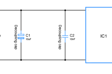
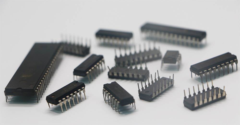
Look at an IC on any PCB layout, and you’re bound to find a few capacitors nearby. (Image source)
How to Use Decoupling Capacitors
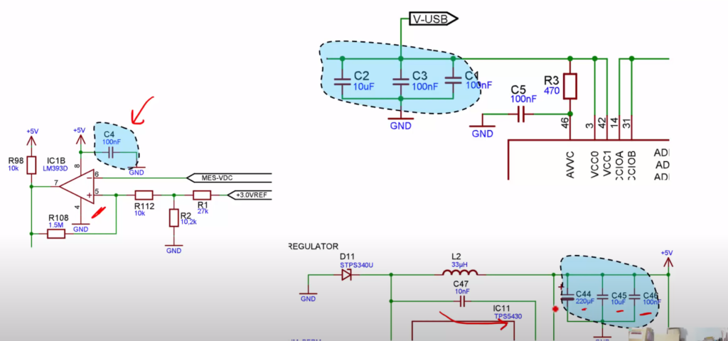
Check out the schematic below; it shows off a typical application of how you might use decoupling capacitors when placed next to an IC. As you can see, you’ve got a 10uF capacitor sitting the furthest away from the IC, which helps to smooth out any low-frequency changes in an input voltage.
A typical application of using decoupling capacitors next to an IC. (Image source)
And then you have the 0.1uF capacitor placed closest to the IC. This one will help to smooth out any of the high-frequency noise in your circuit. When you combine these two capacitors together, you’ll be delivering a smooth, uninterrupted voltage to your IC to work with. When working with decoupling capacitors in your own design, keep these three things in mind:
Placement. You’ll always want to connect your decoupling capacitors between your power source, whether that’s 5V or 3.3V, and ground.
Distance. You’ll always want to place your decoupling capacitors as close as possible to your IC. The farther away they are, the less effective they’ll be.
Ratings. As a general guideline, we always recommend adding a single 100nF ceramic capacitor and a larger 0.1-10uF electrolytic capacitor for each integrated circuit on your board.
Saving Your Integrated Circuit’s Life
There you go, everything you might need to know about what decoupling capacitors are in only 5 minutes in today’s Electronic Byte. Integrated circuits are a sensitive bunch, and without a smooth power source, you’ll likely be troubleshooting skipped instructions and other strange behaviors. By throwing a set of decoupling capacitors next to one of your ICs, you’ll ensure that they’re always getting a smooth input voltage, regardless of what kind of electrical noise is on your PCB.
Capacitor are widely known for its timing properties, however filtering is another important property of this component that has been used by circuit designers.
DECOUPLING AND COUPLING CAPACITORS:
Power supplies are really unstable, you should always keep that in your mind. Every power supply when comes to practical life will not be stable and often the output voltage obtained will be fluctuating at least few hundred mill volts. We often cannot allow this kind of voltage fluctuations while powering our circuit. Because voltage fluctuations may make the circuit to misbehave and especially when comes to microcontroller boards there is even a risk of MCU skipping a instruction which can result in devastating results.
In order to overcome this designers will add a capacitor in parallel and close to the power supply while designing circuit. If you know how capacitor works you will know, by doing this capacitor will start charging from the power supply until it reaches the level of VCC. Once the Vcc level is reached current will no more pass through the cap and stops charging. The capacitor will hold this charge until there is a drop in voltage from the power supply. When voltage from the supply, voltage across the plates of a capacitor will not change instantaneously. At this instant Capacitor will immediately compensate for the voltage drop from the supply by providing current from itself.
Similarly when the voltage fluctuates otherwise creating a voltage spike in the output. Capacitor will start to charge with respect to the spike and then discharge while keeping the voltage across it steady thereby the spike will not reach the digital chip thus ensures steady working.
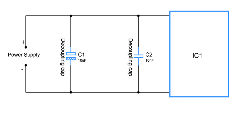
COUPLING CAPACITORS:
These are capacitors that are widely used in amplifier circuits. Unlike the decoupling capacitors will be in the way of an incoming signal. Likewise the role of these capacitors are quite the opposite from the decoupling ones in a circuit. Coupling capacitors block out the low frequency noise or DC element in a signal. This is based on the fact that DC current cannot pass through a capacitor.
The decoupling capacitor is extremely used in Amplifiers since it will curb the DC or low frequency noise in the signal and allowing only high frequency usable signal through it. Although the frequency range of curbing the signal depends on the value of capacitor since reactance of a capacitor varies for different frequency ranges. You may to pick the capacitor that suit your needs.
Higher the frequency you need to allow through your capacitor lower the capacitance value of your Capacitor should be. For example in order to allow a 100Hz signal your capacitor value should be somewhere around 10uF, however for allowing 10Khz signal 10nF will do the job. Again this is just a rough estimate of cap values and you need to calculate the reactance for your frequency signal using the formula 1 / ( 2* Pi * f * c ) and choose the capacitor which offers least reactance to your desired signal.
“Floating state should be always avoided” , we often hear this when designing digital circuits. And it is a golden rule you must follow when designing something that involves digital IC’s and switches. All the digital IC’s operates on a certain logic level and there are many logic families. Out of these TTL and CMOS are pretty much widely known.
These logic levels determines the input voltage in a digital IC to interpret it either as a 1 or a 0. For example with +5V as Vcc voltage level of 5 to 2.8v will be interpreted as Logic 1 and 0 to 0.8v will be interpreted as Logic 0. Anything that falls within this voltage range of 0.9 to 2.7v will be an indeterminate region and the chip will interpret either as a 0 or as a 1 we can’t really tell.
To avoid the above scenario, we use resistors to fix the voltage in the input pins. Pull up resistors to fix the voltage close to Vcc ( voltage drop exists due to current flow ) and Pull down resistors to pull the voltage close to GND pins. This way the floating state in the inputs can be avoided, thus avoid our digital IC’s from behaving incorrectly.
As I said these pull up and pull down resistors will come in handy for Microcontrollers and Digital chips, But do note that many modern MCU’s are equipped with internal Pull up and Pull down resistors which can be activated using the code. So you might check the datasheet for this and choose to either use or eliminate pull up / down resistors accordingly.
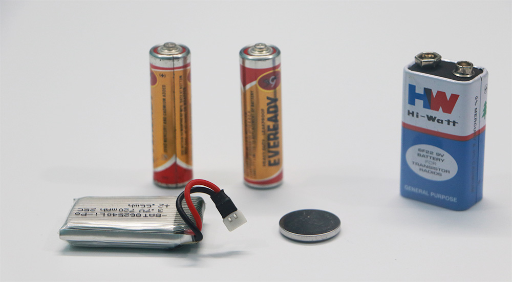
Batteries are a great source to power up your circuit. You will have to choose the battery if you want your design to be mobile. But choosing the right battery might be bit tricky than you actually think. That is because batteries are susceptible to drop their output voltage when their current capacity decreases. Although how far the voltage will drop depends on the type of battery you use ( Lithium ion, Lead acid, Alkaline batteries etc ), there is one good rule of thumb you should always remember.
Always use the battery that has 1.5 times capacity of the current you actually need to run your circuit for a given period of time. Let’s consider that I need to run a 12v motor along with its driver circuit for about 4 hours. The motor itself consumes 150mA and 50mA by driver circuit. So on the whole the entire block consumes 200mA. If I need to run the above circuit for about 4 hours then current required should be
200mA x 4 = 800mA
For this case you should be choosing a battery capacity of 1.2Ah. This is because Lithium ion batteries tend to drop their voltages when the current capacity drops to 20% of their total capacity. This means voltage will drop from 12v to somewhere around 9v when the current capacity drops to 240mA in Lithium battery. Here our circuit consumes 800mA for four hours as denoted above which leaves 400mA or 27% current capacity in the battery. Considering the losses this wiggle room should keep our circuit up and running and prevent damage of batteries as well.
Circuit designing by itself can be pretty daunting but its is something very similar to building a house. Take any circuit you could probably find two or three building blocks in it which are put together to function as unit to perform the intended task.
Here is few of these individual circuit blocks – Voltage dividers, RC elements, RLC elements, Amplifier, multivibrators, Switches, Darlington transistor arrays, rectifiers, regulators, counters, registers, multiplexers.
To design circuits you need to have understanding on these basic building blocks on how it works and methods to build them. Once you possess fair knowledge on these blocks you will find yourself in a good position to design circuits for the intended purposes. But remember putting these elements together may not be straightforward and take practice to do so but this will give you a head start in making your circuit design.
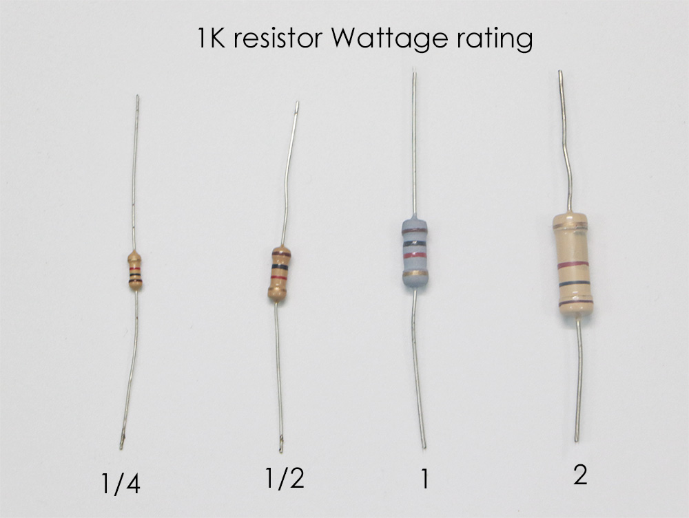
5) RESISTOR WATTAGE:
This is the thing which is commonly ignored by many novice designers and it is very important to take this into consideration when designing your circuits. Resistors as we know resist current flow through it at a given voltage. When this happens electrical energy will experience a loss in the form of heat.
Wattage rating or power rating of a resistor indicate the amount of power it can safely dissipate in the form of heat. When power dissipated exceeds the rated wattage it will result in smoking of resistor and potentially can damage the entire circuit. So Wattage rating of a resistor is equally important as their resistance values.
Let’s say you want to use a resistor in a circuit where it allows 100mA of current at 9V, so the total power here will be P=VI or P = 50mA * 9V = 0.45Watts. In this case we should choose a resistor with wattage rating of at least ½ or 0.5 Watt resistor.
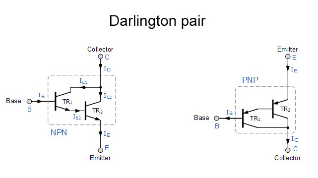
6) USING TRANSISTOR ARRAYS:
Transistors the most valuable component used in electronics. The main two functions of a transistor is to act as a switch and as an amplifier. But when using transistor as a switch we might come across a situation where the gain of our transistor is not sufficient enough to drive the load connected to it.
In these cases we use a special transistor arrangement called Darlington pair, where transistors are connected together as shown above. The transistors can be either same or different. The darlington transistor pairs give high current gain which ranges in around 1000 whereas a single transistor is only capable of giving gain from 100 to 200. Thus this allows a small base current to switch large loads.
Darlington transistor pairs are extremely useful where your single transistor couldn’t drive the load and you could add another transistor to it and drive the desired load.
Over killing a circuit design often occurs among designers where they try and integrate as many components as possible to complete the design. This is not really necessary since plenty of modern cost effective MCU’s in the market are quite capable of replacing the parts making your design less bulky and cost effective. Combining right analog parts or digital chips with Microcontroller will reduce the size of your circuit and increase the efficiency quite dramatically.
Modern microcontroller’s comes in small packages ( 6 pins, 8 pins ) and have features like Timer, PWM, Serial communication, ADC and much more. Occupying less space with some advanced features we must look for spots in our circuit to substitute bulk chips / components with these MCU’s to achieve cost versus performance benefits in our design.
8) PWM SIGNALS:
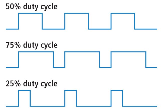
PWM signals have wide range of applications, however for this tip we are going to see its ability on saving power on LED and motor circuits. As you know PWM is a type of modulation where you can modify the width of pulse. For a 60hz PWM signal with 70% duty cycle, pulse will stay ON for 70% and 30% will be off for the total time period.
When we use these signals to drive a LED or motor, current will flow only for 70% of their total time and no current will go through during the OFF time. This happens since the PWM signal at 60HZ is too fast and when we drive LED’s or motor which are pretty slow to react to this frequency. Hence they will give an impression that it is staying ON all the time meanwhile reducing the power consumed.
To explain this better consider a 60hZ & 70% duty PWM signal driving a LED with forward voltage of 3v and 30mA current consumption. So the power consumed will be
3v * 30mA = 90mW
Now since the LED is ON only for 70% of the time, actual power consumed will be 90mW * 70 / 100 = 63mW. So when you design a LED or motor circuit especially if it is a heavy current draw one dedicate some space for PWM generation circuitry, this will save you a lot of power. And PWM signals can be generated from simple 555’s to MCU’s pick anything that you see fit.
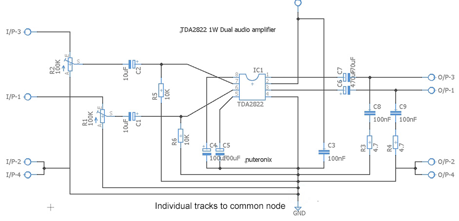
9) INDIVIDUAL TRACKS FOR SIGNAL REFERENCES:
When designing a PCB or wiring a circuit, make sure all signal references have an individual trace back to the common node or ground. When you have many chips in your design, connect the common or ground pins of these chips individually to common node rather than interconnecting with them with each other and then connecting it with the common node.
Tying the signal references otherwise will have negative effects in our circuit. This will result in hum and noise in analog amplifier circuits. This also applies to wiring of input or output jacks, tone and volume controls and switches.
10) CHOOSING THE RIGHT COMPONENT:
This is one of the most challenging task every designer will come across. Many designers will stick to the parts they have used in the past in their designs or use components from the circuits they find in the internet. This might sound like a workable approach but it will be definitely not optimum, you must choose your parts as per your requirements.
To do this websites of component vendors like Mouser, Digikey, Arrow, Avnet etc will be of great help. Almost all the websites have advance part search index where can find parts based on their characteristics. The options listed can be quite overwhelming but ultimately it will do the job.
You will get to refine the search with specifications like package, electrical characteristics, dimensions, cost which will fit your requirement and you will ultimately find the best suited part as per your circuit design.
FINAL WORDS:
I want to thank Ron Hoffman, Jennifer and Vlad for sharing their inputs which helped me in writing this article. The above 10 tips are very few and am quite sure there are plenty of handy tips from other fellow designers. Please share it us via the comment box below, am happy to add them in the article as well. Hope this article would have helped you with circuit designing, looking forward to hear your thoughts and suggestions.
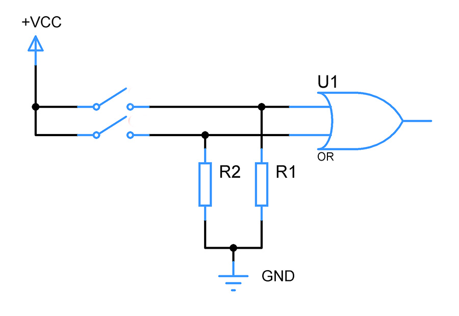
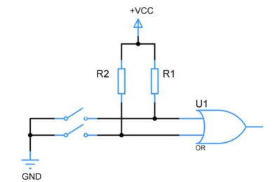
These are common resistors that connects the digital input pins to VCC or Ground. The purpose of these resistors is to bring up the input pins equivalent to the voltage of Ground or VCC. Refer the above circuit diagram the resistors R1 and R2 is the Pull up resistors. These resistors are pulling up the voltage of input pins to the level of VCC.
Now take a look at the above circuit diagram, here the resistors R1 and R2 act as pull down resistors. These resistors are pulling down the voltage of inputs pins close to the level of GND.
WHY USE PULL UP OR PULL DOWN RESISTORS:
In short the purpose of Pull up or Pull down resistor to give keep the input of digital pins at a stable state – 1 in case of Pull up resistor and 0 in case of Pull down resistor. To explain this further, we need to understand about Logic families and how each family differs from each other.
LOGIC LEVEL:
Logic level is nothing but the voltage range which decides how an input or output in a digital circuit is interpreted either as a “1” – high state or “0” – low state. There are many logic family exists in digital systems. TTl, CMOS, RTL, DTL are few of the families and out of which TTL and CMOS are quite famous and commonly used.
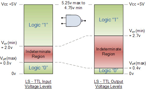
The above image shows the logic level diagram of TTL logic family of +5Vcc. As you can observe in both output and input diagrams, there is a voltage range for each logic states. Referring to input voltage levels, you can observe
For the Gate to read Logic 1 – Input voltage range must be between 2v to 5v
For the Gate to read Logic 0 – Input voltage range must be between 0 to 0.8v
The indeterminate region is the pitfall, this means when input voltage falls between from 0.8 to 2v the Gate will not understand it and it will act in an undesirable manner. Output could be either 0 or 1 and we can’t predict them.
The last case is too bad for designing a digital circuit, since it may make the entire circuit to fail and your design will do no good.
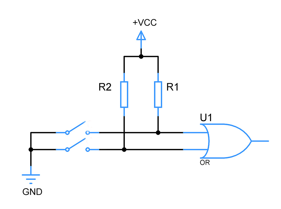
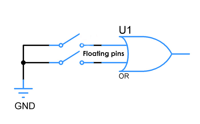
FLOATING STATE:
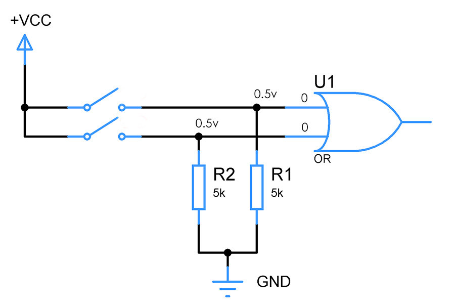
Now take a look at the above circuit where a switch is connected to the input pins of OR gate. When the switch is not connected the pins are said to be in a floating state which means no defined voltage is exhibited in it. In this instant Electrical noise or EM waves from the surrounding will induce some voltage in these pins and as a result there are high chances that the input voltage falls into that indeterminate region of 0.8 to 2v and thereby pushing our entire system to fail. In worst cases the noises and EM waves will produce fluctuating voltage making the entire system unstable.
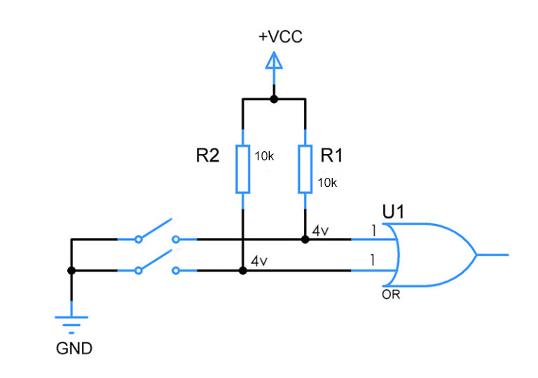
To get rid of this above scenario add a resistor to both the input pins and connect them to Vcc. By doing this the input pins voltage will be pulled up and the voltage will be nearly equivalent to Vcc. This makes the logic gate to detect the input voltage as Logic 1 and act accordingly.
CALCULATING THE RESISTOR VALUE:
Every digital input pin consume some current and has some internal impedance in it. Due to these reasons voltage drop exists across these Pull up resistors. So when choosing the resistor value we should make sure
That the resistor is not too high so that it won’t allow enough current for input pin to operate
Too small so that excess current flows through and lead to short circuit.
PULL UP RESISTORS:
Let’s assume that our digital pin of OR gate consumes 100uA at +5Vcc. I have choosen 4v as Pull up voltage for the purpose of choosing resistor since it will give some nice room from 2v beyond which lies the indeterminate region. You cannot choose 5v since there will be some voltage drop in across the resistor as stated above, so it’s safe to choose less than the level of Vcc. Applying ohms law with these values,
R = 5 – 4 / 100uA
= 1 / 100uA
= 10Kohms
PULL DOWN RESISTORS:
With the above current of 100uA of consumption, am going to choose the pull down voltage of 0.5v since it gives a room from the 0.8v above which the input enters the indeterminate region. Applying ohms law here will give resistor value of
R = 0.5v / 100uA
= 5Kohms
NOTE:
Check the datasheet for input current and input impedence of your digital chip and perform the above calculation to find the perfect pull up or pull down resistor for your digital circuit.
Never attempt to try the above setup without resistors, you will end up shorting your power supply since closing switch without resistors will lead to excess current flow since no impedance is available.