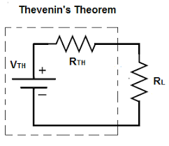
Thevenin’s Theorem states that it is possible to simplify any linear circuit, no matter how complex, to an equivalent circuit with just a single voltage source and series resistance connected to a load. The qualification of “linear” is identical to that found in the Superposition Theorem, where all the underlying equations must be linear (no exponents or roots). If we’re dealing with passive components (such as resistors, and later, inductors and capacitors), this is true. However, there are some components (especially certain gas-discharge and semiconductor components) which are nonlinear: that is, their opposition to current changes with voltage and/or current. As such, we would call circuits containing these types of components, nonlinear circuits.
Thevenin’s Theorem in Power Systems
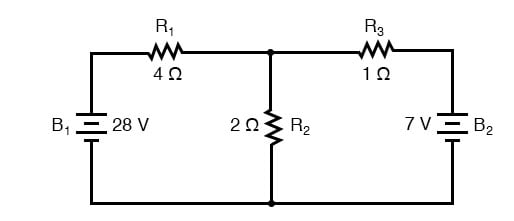
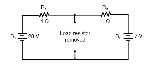
Thevenin’s Theorem is especially useful in analyzing power systems and other circuits where one particular resistor in the circuit (called the “load” resistor) is subject to change, and re-calculation of the circuit is necessary with each trial value of load resistance, to determine the voltage across it and current through it. Let’s take another look at our example circuit:
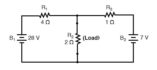
Let’s suppose that we decide to designate R2 as the “load” resistor in this circuit. We already have four methods of analysis at our disposal (Branch Current, Mesh Current, Millman’s Theorem, and Superposition Theorem) to use in determining the voltage across R2 and current through R2, but each of these methods are time-consuming. Imagine repeating any of these methods over and over again to find what would happen if the load resistance changed (changing load resistance is very common in power systems, as multiple loads get switched on and off as needed. the total resistance of their parallel connections changing depending on how many are connected at a time). This could potentially involve a lot of work!
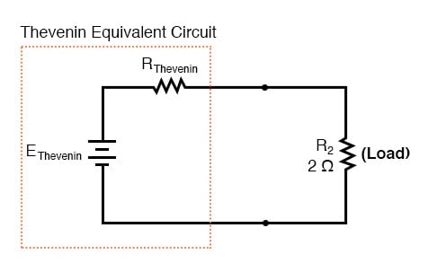
Thevenin Equivalent Circuit
Thevenin’s Theorem makes this easy by temporarily removing the load resistance from the original circuit and reducing what’s left to an equivalent circuit composed of a single voltage source and series resistance. The load resistance can then be re-connected to this “Thevenin equivalent circuit” and calculations carried out as if the whole network were nothing but a simple series circuit:
. . . after Thevenin conversion . . .
The “Thevenin Equivalent Circuit” is the electrical equivalent of B1, R1, R3, and B2 as seen from the two points where our load resistor (R2) connects.
The Thevenin equivalent circuit, if correctly derived, will behave exactly the same as the original circuit formed by B1, R1, R3, and B2. In other words, the load resistor (R2) voltage and current should be exactly the same for the same value of load resistance in the two circuits. The load resistor R2 cannot “tell the difference” between the original network of B1, R1, R3, and B2, and the Thevenin equivalent circuit of EThevenin, and RThevenin, provided that the values for EThevenin and RThevenin have been calculated correctly.
The advantage in performing the “Thevenin conversion” to the simpler circuit, of course, is that it makes load voltage and load current so much easier to solve than in the original network. Calculating the equivalent Thevenin source voltage and series resistance is actually quite easy. First, the chosen load resistor is removed from the original circuit, replaced with a break (open circuit):
Determine Thevenin Voltage
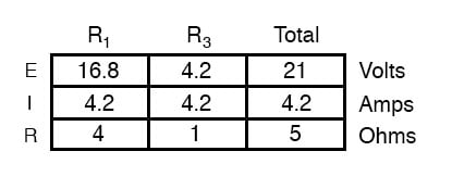
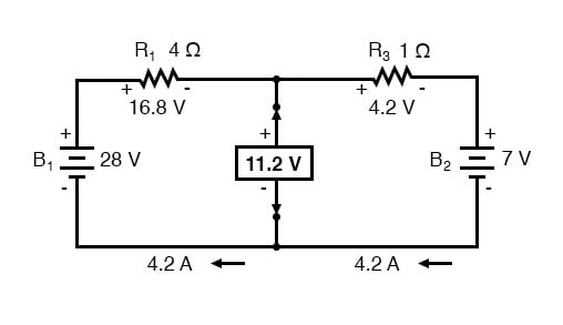
Next, the voltage between the two points where the load resistor used to be attached is determined. Use whatever analysis methods are at your disposal to do this. In this case, the original circuit with the load resistor removed is nothing more than a simple series circuit with opposing batteries, and so we can determine the voltage across the open load terminals by applying the rules of series circuits, Ohm’s Law, and Kirchhoff’s Voltage Law:
The voltage between the two load connection points can be figured from one of the battery’s voltages and one of the resistor’s voltage drops and comes out to 11.2 volts. This is our “Thevenin voltage” (EThevenin) in the equivalent circuit:
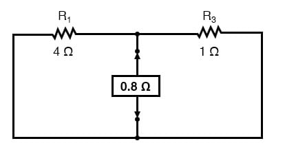
Determine Thevenin Series Resistance
To find the Thevenin series resistance for our equivalent circuit, we need to take the original circuit (with the load resistor still removed), remove the power sources (in the same style as we did with the Superposition Theorem: voltage sources replaced with wires and current sources replaced with breaks), and figure the resistance from one load terminal to the other:
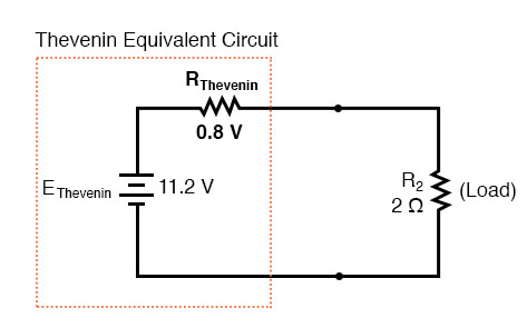
With the removal of the two batteries, the total resistance measured at this location is equal to R1 and R3 in parallel: 0.8 Ω. This is our “Thevenin resistance” (RThevenin) for the equivalent circuit:
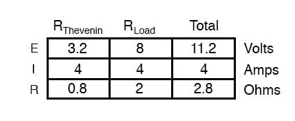
Determine The Voltage Across The Load Resistor
With the load resistor (2 Ω) attached between the connection points, we can determine the voltage across it and current through it as though the whole network were nothing more than a simple series circuit:
Notice that the voltage and current figures for R2 (8 volts, 4 amps) are identical to those found using other methods of analysis. Also notice that the voltage and current figures for the Thevenin series resistance and the Thevenin source (total) do not apply to any component in the original, complex circuit. Thevenin’s Theorem is only useful for determining what happens to a single resistor in a network: the load.
The advantage, of course, is that you can quickly determine what would happen to that single resistor if it were of a value other than 2 Ω without having to go through a lot of analysis again. Just plug in that other value for the load resistor into the Thevenin equivalent circuit and a little bit of series circuit calculation will give you the result.
5.5 example
REVIEW:
Thevenin’s Theorem is a way to reduce a network to an equivalent circuit composed of a single voltage source, series resistance, and series load.
Steps to follow for Thevenin’s Theorem:
Find the Thevenin source voltage by removing the load resistor from the original circuit and calculating the voltage across the open connection points where the load resistor used to be.
Find the Thevenin resistance by removing all power sources in the original circuit (voltage sources shorted and current sources open) and calculating total resistance between the open connection points.
Draw the Thevenin equivalent circuit, with the Thevenin voltage source in series with the Thevenin resistance. The load resistor re-attaches between the two open points of the equivalent circuit.
Analyze voltage and current for the load resistor following the rules for series circuits.
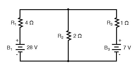
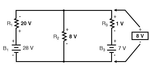
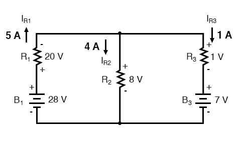
In Millman’s Theorem, the circuit is re-drawn as a parallel network of branches, each branch containing a resistor or series battery/resistor combination. Millman’s Theorem is applicable only to those circuits which can be redrawn accordingly. Here again, is our example circuit used for the last two analysis methods:
And here is that same circuit, re-drawn for the sake of applying Millman’s Theorem:
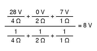
By considering the supply voltage within each branch and the resistance within each branch, Millman’s Theorem will tell us the voltage across all branches. Please note that I’ve labeled the battery in the rightmost branch as “B3” to clearly denote it as being in the third branch, even though there is no “B2” in the circuit!
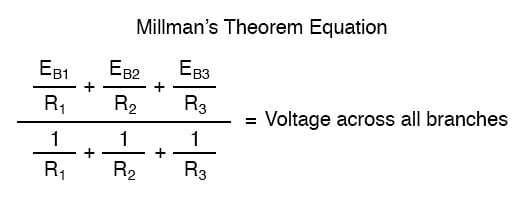
Millman’s Theorem Equation
Millman’s Theorem is nothing more than a long equation, applied to any circuit drawn as a set of parallel-connected branches, each branch with its own voltage source and series resistance:
Substituting actual voltage and resistance figures from our example circuit for the variable terms of this equation, we get the following expression:
The final answer of 8 volts is the voltage seen across all parallel branches, like this:
The polarity of all voltages in Millman’s Theorem is referenced to the same point. In the example circuit above, I used the bottom wire of the parallel circuit as my reference point, and so the voltages within each branch (28 for the R1 branch, 0 for the R2 branch, and 7 for the R3 branch) were inserted into the equation as positive numbers. Likewise, when the answer came out to 8 volts (positive), this meant that the top wire of the circuit was positive with respect to the bottom wire (the original point of reference). If both batteries had been connected backward (negative end up and positive ends down), the voltage for branch 1 would have been entered into the equation as -28 volts, the voltage for branch 3 as -7 volts, and the resulting answer of -8 volts would have told us that the top wire was negative with respect to the bottom wire (our initial point of reference).
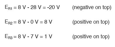
Solving for Resistor Voltage Drops
To solve for resistor voltage drops, the Millman voltage (across the parallel network) must be compared against the voltage source within each branch, using the principle of voltages adding in series to determine the magnitude and polarity of the voltage across each resistor:
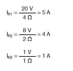
Solving for Branch Currents
To solve for branch currents, each resistor voltage drop can be divided by its respective resistance (I=E/R):
Determining the Direction of Current
The direction of current through each resistor is determined by the polarity across each resistor, not by the polarity across each battery, as the current can be forced back through a battery, as is the case with B3 in the example circuit. This is important to keep in mind since Millman’s Theorem doesn’t provide as direct an indication of “wrong” current direction as does the Branch Current or Mesh Current methods. You must pay close attention to the polarities of resistor voltage drops as given by Kirchhoff’s Voltage Law, determining the direction of currents from that.
Millman’s Theorem is very convenient for determining the voltage across a set of parallel branches, where there are enough voltage sources present to preclude solution via regular series-parallel reduction method. It also is easy in the sense that it doesn’t require the use of simultaneous equations. However, it is limited in that it only applied to circuits which can be re-drawn to fit this form. It cannot be used, for example, to solve an unbalanced bridge circuit. And, even in cases where Millman’s Theorem can be applied, the solution of individual resistor voltage drops can be a bit daunting to some, the Millman’s Theorem equation only providing a single figure for branch voltage.
As you will see, each network analysis method has its own advantages and disadvantages. Each method is a tool, and there is no tool that is perfect for all jobs. The skilled technician, however, carries these methods in his or her mind like a mechanic carries a set of tools in his or her toolbox. The more tools you have equipped yourself with, the better prepared you will be for any eventuality.
Electronic Byte: What are Decoupling Capacitors, in Only 5 Minutes
It’s pretty standard for beginner electronic designers to forget just how unstable input voltages can be, despite how sturdy that power supply might look. And when you’re working with microcontrollers or microprocessors in your digital circuit, the slightest fluctuation in your voltage can lead to undesired results. So what can you do to keep your ICs running with smooth, clean voltage? Use decoupling capacitors! Here’s what they are, and how to use them in today’s Electronic Byte.
What Are Decoupling Capacitors
A decoupling capacitor, also referred to as a bypass capacitor, acts as a kind of energy reservoir. You’ll find these guys commonly placed as close as possible to an integrated circuit (IC) on a PCB layout. Once fully charged, their job is to simply oppose any unexpected change in your input voltages from a power supply. When a decoupling capacitor is in place, it will do one of two things:
If the input voltage drops, then a decoupling capacitor will be able to provide enough power to an IC to keep the voltage stable.
If the voltage increases, then a decoupling capacitor will be able to absorb the excess energy trying to flow through to the IC, which again keeps the voltage stable.
All of this is needed because there’s a ton of electrical noise on a typical circuit board, and the steady 5V that we think we have flowing all over the place is actually jumping around as it moves from component to component.
Some components like integrated circuits rely on their input voltage being as steady as possible, so when you place a decoupling capacitor next to an IC, you’ll be able to protect those sensitive chips by filtering out any excess noise and creating a nice, steady source of power. What happens if you don’t use decoupling capacitors next to your IC? Well, you’ll likely wind up with a processor that starts skipping instructions and behaving abnormally.
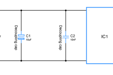
Look at an IC on any PCB layout, and you’re bound to find a few capacitors nearby. (Image source)
How to Use Decoupling Capacitors
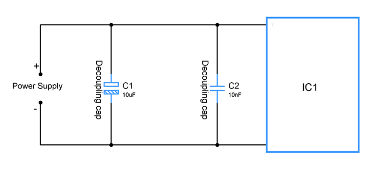
Check out the schematic below; it shows off a typical application of how you might use decoupling capacitors when placed next to an IC. As you can see, you’ve got a 10uF capacitor sitting the furthest away from the IC, which helps to smooth out any low-frequency changes in an input voltage.
A typical application of using decoupling capacitors next to an IC. (Image source)
And then you have the 0.1uF capacitor placed closest to the IC. This one will help to smooth out any of the high-frequency noise in your circuit. When you combine these two capacitors together, you’ll be delivering a smooth, uninterrupted voltage to your IC to work with. When working with decoupling capacitors in your own design, keep these three things in mind:
Placement. You’ll always want to connect your decoupling capacitors between your power source, whether that’s 5V or 3.3V, and ground.
Distance. You’ll always want to place your decoupling capacitors as close as possible to your IC. The farther away they are, the less effective they’ll be.
Ratings. As a general guideline, we always recommend adding a single 100nF ceramic capacitor and a larger 0.1-10uF electrolytic capacitor for each integrated circuit on your board.
Saving Your Integrated Circuit’s Life
There you go, everything you might need to know about what decoupling capacitors are in only 5 minutes in today’s Electronic Byte. Integrated circuits are a sensitive bunch, and without a smooth power source, you’ll likely be troubleshooting skipped instructions and other strange behaviors. By throwing a set of decoupling capacitors next to one of your ICs, you’ll ensure that they’re always getting a smooth input voltage, regardless of what kind of electrical noise is on your PCB.
Capacitor are widely known for its timing properties, however filtering is another important property of this component that has been used by circuit designers.
DECOUPLING AND COUPLING CAPACITORS:
Power supplies are really unstable, you should always keep that in your mind. Every power supply when comes to practical life will not be stable and often the output voltage obtained will be fluctuating at least few hundred mill volts. We often cannot allow this kind of voltage fluctuations while powering our circuit. Because voltage fluctuations may make the circuit to misbehave and especially when comes to microcontroller boards there is even a risk of MCU skipping a instruction which can result in devastating results.
In order to overcome this designers will add a capacitor in parallel and close to the power supply while designing circuit. If you know how capacitor works you will know, by doing this capacitor will start charging from the power supply until it reaches the level of VCC. Once the Vcc level is reached current will no more pass through the cap and stops charging. The capacitor will hold this charge until there is a drop in voltage from the power supply. When voltage from the supply, voltage across the plates of a capacitor will not change instantaneously. At this instant Capacitor will immediately compensate for the voltage drop from the supply by providing current from itself.
Similarly when the voltage fluctuates otherwise creating a voltage spike in the output. Capacitor will start to charge with respect to the spike and then discharge while keeping the voltage across it steady thereby the spike will not reach the digital chip thus ensures steady working.
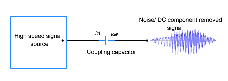
COUPLING CAPACITORS:
These are capacitors that are widely used in amplifier circuits. Unlike the decoupling capacitors will be in the way of an incoming signal. Likewise the role of these capacitors are quite the opposite from the decoupling ones in a circuit. Coupling capacitors block out the low frequency noise or DC element in a signal. This is based on the fact that DC current cannot pass through a capacitor.
The decoupling capacitor is extremely used in Amplifiers since it will curb the DC or low frequency noise in the signal and allowing only high frequency usable signal through it. Although the frequency range of curbing the signal depends on the value of capacitor since reactance of a capacitor varies for different frequency ranges. You may to pick the capacitor that suit your needs.
Higher the frequency you need to allow through your capacitor lower the capacitance value of your Capacitor should be. For example in order to allow a 100Hz signal your capacitor value should be somewhere around 10uF, however for allowing 10Khz signal 10nF will do the job. Again this is just a rough estimate of cap values and you need to calculate the reactance for your frequency signal using the formula 1 / ( 2* Pi * f * c ) and choose the capacitor which offers least reactance to your desired signal.
“Floating state should be always avoided” , we often hear this when designing digital circuits. And it is a golden rule you must follow when designing something that involves digital IC’s and switches. All the digital IC’s operates on a certain logic level and there are many logic families. Out of these TTL and CMOS are pretty much widely known.
These logic levels determines the input voltage in a digital IC to interpret it either as a 1 or a 0. For example with +5V as Vcc voltage level of 5 to 2.8v will be interpreted as Logic 1 and 0 to 0.8v will be interpreted as Logic 0. Anything that falls within this voltage range of 0.9 to 2.7v will be an indeterminate region and the chip will interpret either as a 0 or as a 1 we can’t really tell.
To avoid the above scenario, we use resistors to fix the voltage in the input pins. Pull up resistors to fix the voltage close to Vcc ( voltage drop exists due to current flow ) and Pull down resistors to pull the voltage close to GND pins. This way the floating state in the inputs can be avoided, thus avoid our digital IC’s from behaving incorrectly.
As I said these pull up and pull down resistors will come in handy for Microcontrollers and Digital chips, But do note that many modern MCU’s are equipped with internal Pull up and Pull down resistors which can be activated using the code. So you might check the datasheet for this and choose to either use or eliminate pull up / down resistors accordingly.
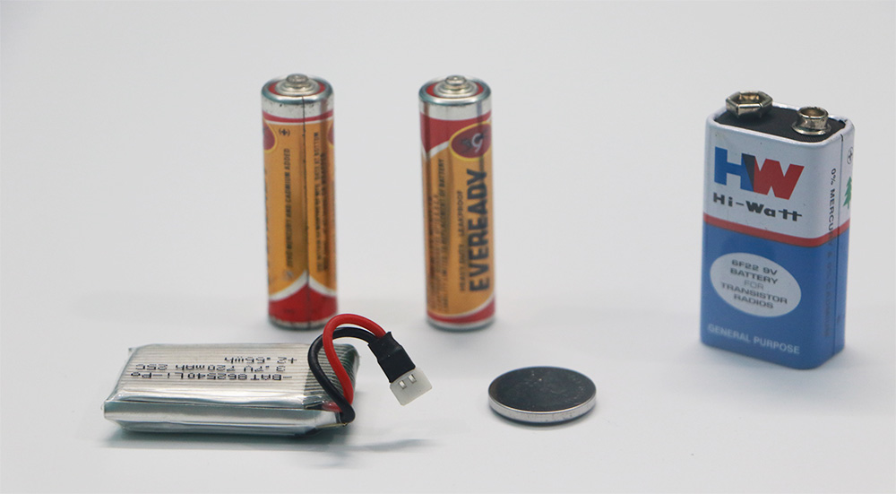
Batteries are a great source to power up your circuit. You will have to choose the battery if you want your design to be mobile. But choosing the right battery might be bit tricky than you actually think. That is because batteries are susceptible to drop their output voltage when their current capacity decreases. Although how far the voltage will drop depends on the type of battery you use ( Lithium ion, Lead acid, Alkaline batteries etc ), there is one good rule of thumb you should always remember.
Always use the battery that has 1.5 times capacity of the current you actually need to run your circuit for a given period of time. Let’s consider that I need to run a 12v motor along with its driver circuit for about 4 hours. The motor itself consumes 150mA and 50mA by driver circuit. So on the whole the entire block consumes 200mA. If I need to run the above circuit for about 4 hours then current required should be
200mA x 4 = 800mA
For this case you should be choosing a battery capacity of 1.2Ah. This is because Lithium ion batteries tend to drop their voltages when the current capacity drops to 20% of their total capacity. This means voltage will drop from 12v to somewhere around 9v when the current capacity drops to 240mA in Lithium battery. Here our circuit consumes 800mA for four hours as denoted above which leaves 400mA or 27% current capacity in the battery. Considering the losses this wiggle room should keep our circuit up and running and prevent damage of batteries as well.
Circuit designing by itself can be pretty daunting but its is something very similar to building a house. Take any circuit you could probably find two or three building blocks in it which are put together to function as unit to perform the intended task.
Here is few of these individual circuit blocks – Voltage dividers, RC elements, RLC elements, Amplifier, multivibrators, Switches, Darlington transistor arrays, rectifiers, regulators, counters, registers, multiplexers.
To design circuits you need to have understanding on these basic building blocks on how it works and methods to build them. Once you possess fair knowledge on these blocks you will find yourself in a good position to design circuits for the intended purposes. But remember putting these elements together may not be straightforward and take practice to do so but this will give you a head start in making your circuit design.
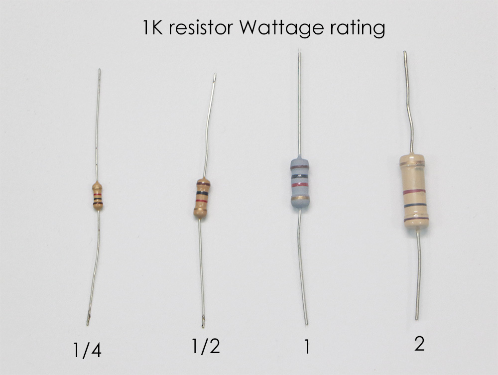
5) RESISTOR WATTAGE:
This is the thing which is commonly ignored by many novice designers and it is very important to take this into consideration when designing your circuits. Resistors as we know resist current flow through it at a given voltage. When this happens electrical energy will experience a loss in the form of heat.
Wattage rating or power rating of a resistor indicate the amount of power it can safely dissipate in the form of heat. When power dissipated exceeds the rated wattage it will result in smoking of resistor and potentially can damage the entire circuit. So Wattage rating of a resistor is equally important as their resistance values.
Let’s say you want to use a resistor in a circuit where it allows 100mA of current at 9V, so the total power here will be P=VI or P = 50mA * 9V = 0.45Watts. In this case we should choose a resistor with wattage rating of at least ½ or 0.5 Watt resistor.
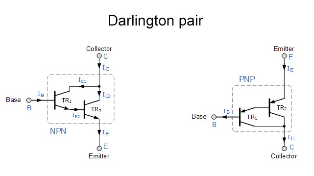
6) USING TRANSISTOR ARRAYS:
Transistors the most valuable component used in electronics. The main two functions of a transistor is to act as a switch and as an amplifier. But when using transistor as a switch we might come across a situation where the gain of our transistor is not sufficient enough to drive the load connected to it.
In these cases we use a special transistor arrangement called Darlington pair, where transistors are connected together as shown above. The transistors can be either same or different. The darlington transistor pairs give high current gain which ranges in around 1000 whereas a single transistor is only capable of giving gain from 100 to 200. Thus this allows a small base current to switch large loads.
Darlington transistor pairs are extremely useful where your single transistor couldn’t drive the load and you could add another transistor to it and drive the desired load.
Over killing a circuit design often occurs among designers where they try and integrate as many components as possible to complete the design. This is not really necessary since plenty of modern cost effective MCU’s in the market are quite capable of replacing the parts making your design less bulky and cost effective. Combining right analog parts or digital chips with Microcontroller will reduce the size of your circuit and increase the efficiency quite dramatically.
Modern microcontroller’s comes in small packages ( 6 pins, 8 pins ) and have features like Timer, PWM, Serial communication, ADC and much more. Occupying less space with some advanced features we must look for spots in our circuit to substitute bulk chips / components with these MCU’s to achieve cost versus performance benefits in our design.
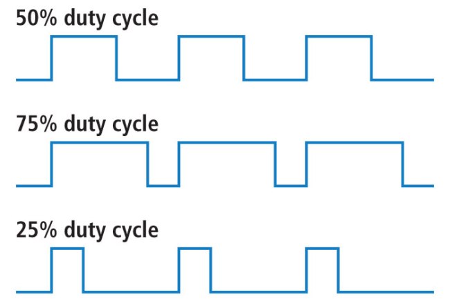
8) PWM SIGNALS:
PWM signals have wide range of applications, however for this tip we are going to see its ability on saving power on LED and motor circuits. As you know PWM is a type of modulation where you can modify the width of pulse. For a 60hz PWM signal with 70% duty cycle, pulse will stay ON for 70% and 30% will be off for the total time period.
When we use these signals to drive a LED or motor, current will flow only for 70% of their total time and no current will go through during the OFF time. This happens since the PWM signal at 60HZ is too fast and when we drive LED’s or motor which are pretty slow to react to this frequency. Hence they will give an impression that it is staying ON all the time meanwhile reducing the power consumed.
To explain this better consider a 60hZ & 70% duty PWM signal driving a LED with forward voltage of 3v and 30mA current consumption. So the power consumed will be
3v * 30mA = 90mW
Now since the LED is ON only for 70% of the time, actual power consumed will be 90mW * 70 / 100 = 63mW. So when you design a LED or motor circuit especially if it is a heavy current draw one dedicate some space for PWM generation circuitry, this will save you a lot of power. And PWM signals can be generated from simple 555’s to MCU’s pick anything that you see fit.
9) INDIVIDUAL TRACKS FOR SIGNAL REFERENCES:
When designing a PCB or wiring a circuit, make sure all signal references have an individual trace back to the common node or ground. When you have many chips in your design, connect the common or ground pins of these chips individually to common node rather than interconnecting with them with each other and then connecting it with the common node.
Tying the signal references otherwise will have negative effects in our circuit. This will result in hum and noise in analog amplifier circuits. This also applies to wiring of input or output jacks, tone and volume controls and switches.
10) CHOOSING THE RIGHT COMPONENT:
This is one of the most challenging task every designer will come across. Many designers will stick to the parts they have used in the past in their designs or use components from the circuits they find in the internet. This might sound like a workable approach but it will be definitely not optimum, you must choose your parts as per your requirements.
To do this websites of component vendors like Mouser, Digikey, Arrow, Avnet etc will be of great help. Almost all the websites have advance part search index where can find parts based on their characteristics. The options listed can be quite overwhelming but ultimately it will do the job.
You will get to refine the search with specifications like package, electrical characteristics, dimensions, cost which will fit your requirement and you will ultimately find the best suited part as per your circuit design.
FINAL WORDS:
I want to thank Ron Hoffman, Jennifer and Vlad for sharing their inputs which helped me in writing this article. The above 10 tips are very few and am quite sure there are plenty of handy tips from other fellow designers. Please share it us via the comment box below, am happy to add them in the article as well. Hope this article would have helped you with circuit designing, looking forward to hear your thoughts and suggestions.
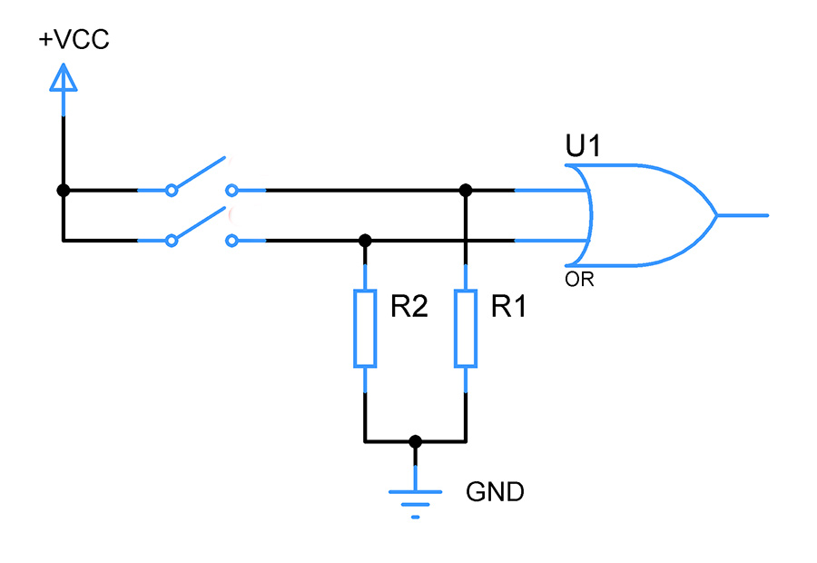
These are common resistors that connects the digital input pins to VCC or Ground. The purpose of these resistors is to bring up the input pins equivalent to the voltage of Ground or VCC. Refer the above circuit diagram the resistors R1 and R2 is the Pull up resistors. These resistors are pulling up the voltage of input pins to the level of VCC.
Now take a look at the above circuit diagram, here the resistors R1 and R2 act as pull down resistors. These resistors are pulling down the voltage of inputs pins close to the level of GND.
WHY USE PULL UP OR PULL DOWN RESISTORS:
In short the purpose of Pull up or Pull down resistor to give keep the input of digital pins at a stable state – 1 in case of Pull up resistor and 0 in case of Pull down resistor. To explain this further, we need to understand about Logic families and how each family differs from each other.
LOGIC LEVEL:
Logic level is nothing but the voltage range which decides how an input or output in a digital circuit is interpreted either as a “1” – high state or “0” – low state. There are many logic family exists in digital systems. TTl, CMOS, RTL, DTL are few of the families and out of which TTL and CMOS are quite famous and commonly used.
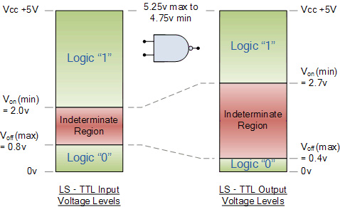
The above image shows the logic level diagram of TTL logic family of +5Vcc. As you can observe in both output and input diagrams, there is a voltage range for each logic states. Referring to input voltage levels, you can observe
For the Gate to read Logic 1 – Input voltage range must be between 2v to 5v
For the Gate to read Logic 0 – Input voltage range must be between 0 to 0.8v
The indeterminate region is the pitfall, this means when input voltage falls between from 0.8 to 2v the Gate will not understand it and it will act in an undesirable manner. Output could be either 0 or 1 and we can’t predict them.
The last case is too bad for designing a digital circuit, since it may make the entire circuit to fail and your design will do no good.
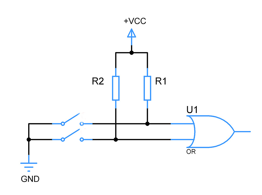
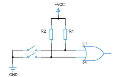
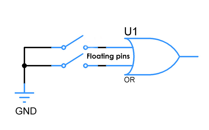
FLOATING STATE:
Now take a look at the above circuit where a switch is connected to the input pins of OR gate. When the switch is not connected the pins are said to be in a floating state which means no defined voltage is exhibited in it. In this instant Electrical noise or EM waves from the surrounding will induce some voltage in these pins and as a result there are high chances that the input voltage falls into that indeterminate region of 0.8 to 2v and thereby pushing our entire system to fail. In worst cases the noises and EM waves will produce fluctuating voltage making the entire system unstable.
To get rid of this above scenario add a resistor to both the input pins and connect them to Vcc. By doing this the input pins voltage will be pulled up and the voltage will be nearly equivalent to Vcc. This makes the logic gate to detect the input voltage as Logic 1 and act accordingly.
CALCULATING THE RESISTOR VALUE:
Every digital input pin consume some current and has some internal impedance in it. Due to these reasons voltage drop exists across these Pull up resistors. So when choosing the resistor value we should make sure
That the resistor is not too high so that it won’t allow enough current for input pin to operate
Too small so that excess current flows through and lead to short circuit.
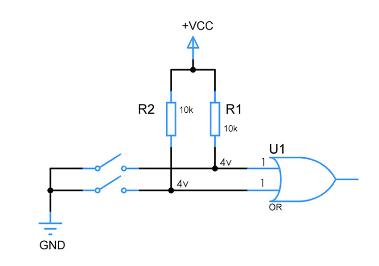
PULL UP RESISTORS:
Let’s assume that our digital pin of OR gate consumes 100uA at +5Vcc. I have choosen 4v as Pull up voltage for the purpose of choosing resistor since it will give some nice room from 2v beyond which lies the indeterminate region. You cannot choose 5v since there will be some voltage drop in across the resistor as stated above, so it’s safe to choose less than the level of Vcc. Applying ohms law with these values,
R = 5 – 4 / 100uA
= 1 / 100uA
= 10Kohms
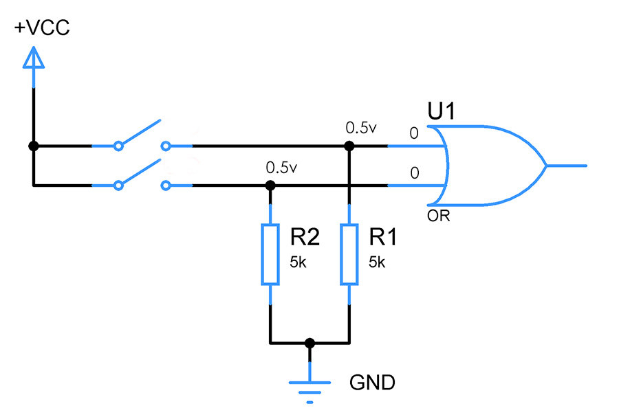
PULL DOWN RESISTORS:
With the above current of 100uA of consumption, am going to choose the pull down voltage of 0.5v since it gives a room from the 0.8v above which the input enters the indeterminate region. Applying ohms law here will give resistor value of
R = 0.5v / 100uA
= 5Kohms
NOTE:
Check the datasheet for input current and input impedence of your digital chip and perform the above calculation to find the perfect pull up or pull down resistor for your digital circuit.
Never attempt to try the above setup without resistors, you will end up shorting your power supply since closing switch without resistors will lead to excess current flow since no impedance is available.
The buck–boost converter is a type of DC-to-DC converter that has an output voltage magnitude that is either greater than or less than the input voltage magnitude. It is equivalent to a flyback converter using a single inductor instead of a transformer.
In this tutorial we will learn how to build and how a DC to DC buck-boost converter works. The circuit is very basic using just one diode, an inductor and a capacitor. The switch will be a MOSFET transistor and to create the PWM signal we will use a 555 timer in the PWM configuration, boost adjustable controller or one Arduino NANO. But first let’s study a little bit of theory. We have the buck-boost converter circuit in the next figure where we can see the switch, inductor and capacitor and of course we add a load to the output.
Buck-Boost converter theory
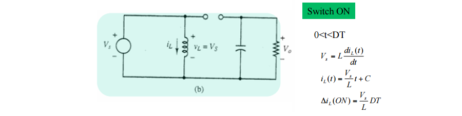
Like the buck and boost converters, the operation of the buck-boost is best understood in terms of the inductor’s “reluctance” to allow rapid change in current. From the initial state in which nothing is charged and the switch is open, the current through the inductor is zero. When the switch is first closed, the blocking diode prevents current from flowing into the right hand side of the circuit, so it must all flow through the inductor. However, since the inductor doesn’t like rapid current change, it will initially keep the current low by dropping most of the voltage provided by the source. Over time, the inductor will allow the current to slowly increase by decreasing its voltage drop. Also during this time, the inductor will store energy in the form of a magnetic field. We have the switch closed so in this case we obtain the current through the inductor using the next formulas.
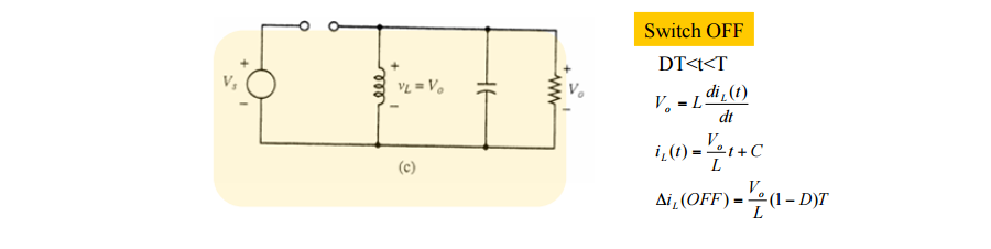
When the switch is opened, current will be reduced as the impedance is higher. The magnetic field previously created will be destroyed to maintain the current towards the load. In this case the voltage across the inductor is the output voltage. So once again using the next figure formulas we obtain the current of the OFF part depending on the duty cycle.
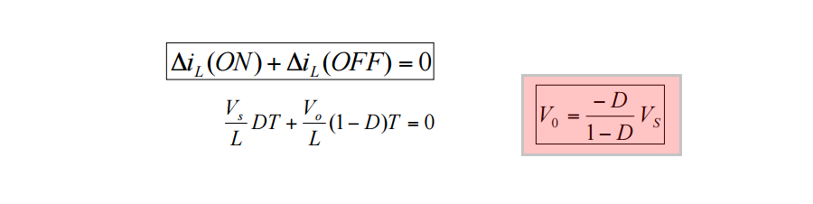
Ok, now if we want to obtain the output depending on the input and the duty cycle of the PWM all we have to do is to make the sum of the On and Off current equal to 0. That means that the On current is equal to the Off current. So that will give us:
So we’ve obtain that the output is depending of the duty cycle disproportionate and also proportional. The duty cycle of the PWM can have values between 0 and 1. In this way we could achive both higher and lower voltages than the onput. That’s why this configuration is called step down-up converter.
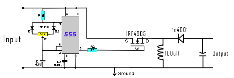
Buck-Boost converter circuit 555 timer
This 555 configuration will create a PWM signal and apply that signal to the MOSFET gate. The circuit works ok but it has a big problem. The output will change if we change the output load because the circuit has no feedback. Ok so we will use the next schematic for our buck-boost converter example. To create the PWM signal we will use the 555 timer with the PWM configuration. With the P1 potentiometer we can change the duty cycle of the PWM signal, and at the same time the output value. For the MOSFET you could use the PMOS IRF4905. You could always try different inductance values for the inductor and see the results.
The input could be up yo 15 volts. Don’t apply higher voltage or you could burn the 555 timer. Connect the PWM (pin 3 of the 555 timer) to the MOSFET (switch) gate. Add an output load and test the circuit. You could obtain output values higher than the input.
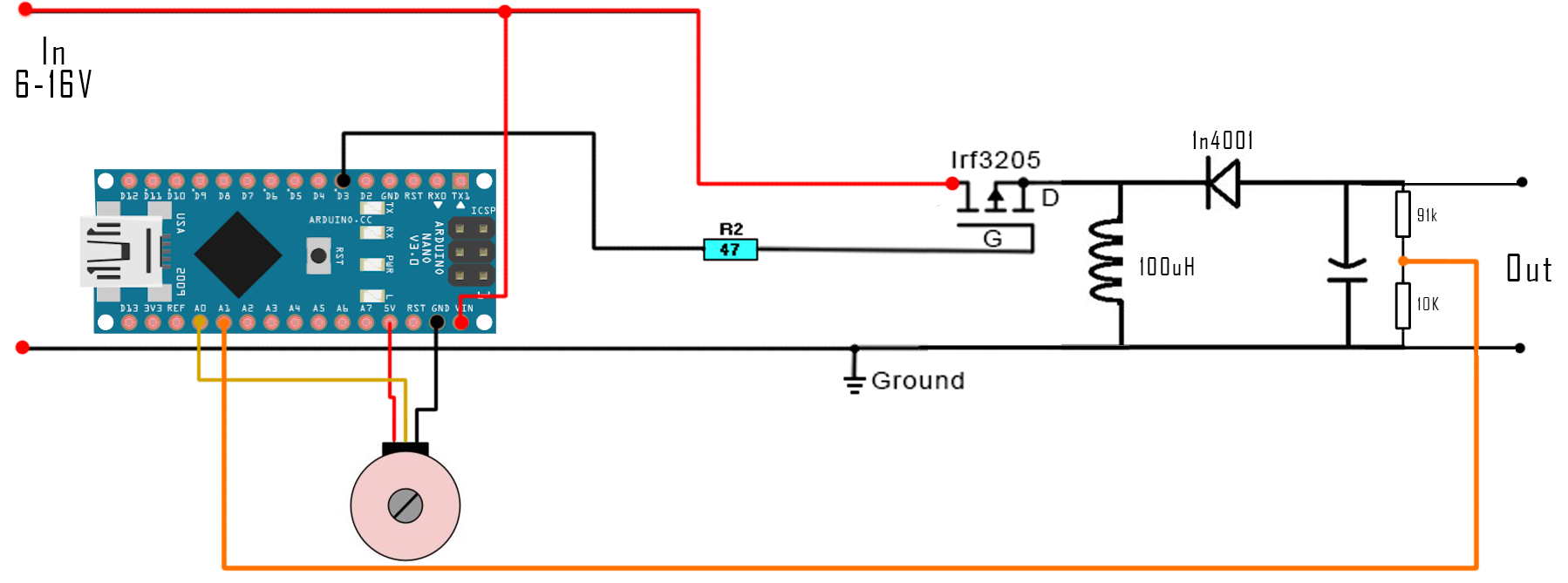
Buck-Boost converter Arduino NANO
Sincerely, this circuit has no sense but to learn. The Arduino NANO already has a 5V linear voltage regulator that will lower the efficiency of the circuit. So the main goal is to learn how the circuit, the feedback and the PWM signal work in order to achive the desired output.
As you can see we have a potentiometer connected to the analog input A0. With this potentiometer we will choose the output value between 1 and 50 volts aprox (your output values may vary). At the output of the circuit we have a voltage divider that will lower the voltage from maximum 50V to under 5 volts because that’s the maximum input voltage of the Arduino ADCs. In the code we compare this two voltages and increase or decrease the PWM width in order to keep the output constant. Just copy and upload the next code to the Arduino for this example.