Audio amplifier and I2S DAC

The sound wave is converted into data through a series of snapshot measurements, or samples. A sample is taken at a particular time in the audio wave, recording amplitude. This information is then converted into digestible, binary data.

The system makes thousands of measurements per second. If we can take tons of measurements extremely quickly with enough possible amplitude values, we can effectively use these snapshots to reconstruct the resolution and complexity of an analog wave.

What is an audio sample rate

The system takes these measurements at a speed called the audio sample rate, measured in kilohertz. The audio sample rate determines the range of frequencies captured in digital audio. In most DAWs, you’ll find an adjustable sample rate in your audio preferences. This controls the sample rate for audio in your project.

What is audio bit depth?

The audio bit depth determines the number of possible amplitude values we can record for each sample. The most common audio bit depths are 16-bit, 24-bit, and 32-bit. Each is a binary term, representing a number of possible values. 

https://www.izotope.com/en/learn/digital-audio-basics-sample-rate-and-bit-depth.html

LM386 Audio Amplifier

I2S DAC

The stated purpose of I2S is to facilitate the development of audio electronics by means of a standardized interface for transmission of digital data among ADCs, DACs, digital filters, digital signal processors, and other types of ICs used in audio systems. It is inherently a two-channel protocol, because it was designed for stereophonic sound
Data is driven on the SD line, the state of the WS line corresponds to the audio channel (right or left) that is currently being transmitted, and the clock line carries the serial clock.

Serial Data (SD)

  • Digital values are transmitted MSb first.
  • Transmitter and receiver do not need to have an agreed-upon word length; the transmitter sends what it has, and the receiver takes what it can use.
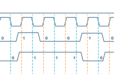
  • New data bits can be clocked out on the rising or falling edge of the clock. However, they must be clocked in on the rising edge, so the more straightforward approach here is the arrangement shown in the diagram below—i.e., we clock data out on the falling edge and we clock it in on the rising edge.
  • The protocol does not include unused clock periods between words; the LSb of one word is followed immediately by the MSb of the next word.

Word Select (WS)

  • A logic low on WS indicates that the word currently being transferred is part of the data stream for the left audio channel; logic high on WS indicates right-channel audio.
  • To facilitate data handling on both the transmitter and the receiver side, the WS signal transitions one clock period before the completion of a data word:

Clock

  • The protocol does not specify a maximum data rate.
  • The clock runs continuously.

UART Protocol

How UART Works?

In UART Serial Communication, the data is transmitted asynchronously i.e. there is no clock or other timing signal involved between the sender and receiver. Instead of clock signal, UART uses some special bits called Start and Stop bits.

These bits are added to the actual data packet at the beginning and end respectively. These additional bits allows the receiving UART to identify the actual data.

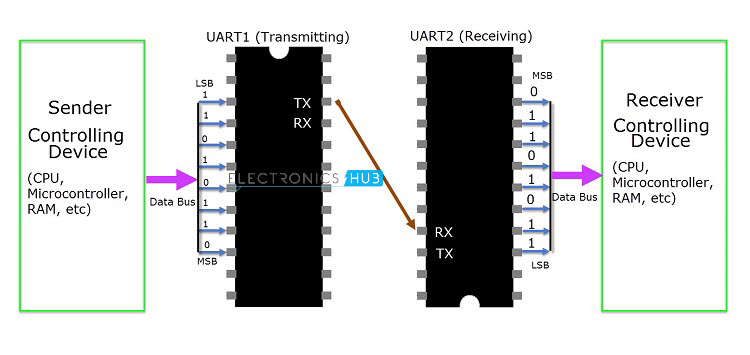
The image above shows a typical UART connection. The transmitting UART receives data from the controlling device through the data bus. The controlling device can be anything like a CPU of a microprocessor or a microcontroller, memory unit like a RAM or ROM, etc. The data received by the transmitting UART from the data bus is parallel data.

To this data, the UART adds Start, Parity and Stop bits in order to convert it into a data packet. The data packet is then converted from parallel to serial with the help of shift register and is transmitted bit – by – bit from the TX pin.

The receiving UART receives this serial data at the RX pin and detects the actual data by identifying the start and stop bits. Parity bit is used to check the integrity of the data.

Up on separating the start, parity and stop bits from the data packet, the data is converted to parallel data with the help of shift register. This parallel data is sent to the controller at the receiving end through a data bus.

Structure of Data Packet or Frame

The data in UART serial communication is organised in to blocks called Packets or Frames. The structure of a typical UART Data Packet or the standard framing of the data is shown in the following image.

Let us see about each piece of the frame.

Start Bit: Start bit is a synchronisation bit that is added before the actual data. Start bit marks the beginning of the data packet. Usually, an idle data line i.e. when the data transmission line is not transmitting any data, it is held at a high voltage level (1).

In order to start the data transfer, the transmitting UART pulls the data line from high voltage level to low voltage level (from 1 to 0). The receiving UART detects this change from high to low on the data line and begins reading the actual data. Usually, there is only one start bit.

Stop Bit: The Stop Bit, as the name suggests, marks the end of the data packet. It is usually two bits long but often only on bit is used. In order to end the transmission, the UART maintains the data line at high voltage (1).

Parity Bit: Parity allows the receiver to check whether the received data is correct or not. Parity is a low – level error checking system and comes in two varieties: Even Parity and Odd Parity. Parity bit is optional and it is actually not that widely used.

Data Bits: Data bits are the actual data being transmitted from sender to receiver. The length of the data frame can be anywhere between 5 and 9 (9 bits if parity is not used and only 8 bits if parity is used). Usually, the LSB is the first bit of data to be transmitted (unless otherwise specified).

Rules of UART

As mentioned earlier, there is no clock signal in UART and the transmitter and receiver must agree on some rules of serial communication for error free transfer of data. The rules include:

  • Synchronisation Bits (Start and Stop bits)
  • Parity Bit
  • Data Bits and
  • Baud Rate

We have seen about synchronisation bits, parity bit and data bits. Another important parameter is the Baud Rate.

Baud Rate: The speed at which the data is transmitted is mentioned using Baud Rate. Both the transmitting UART and Receiving UART must agree on the Baud Rate for a successful data transmission.

Baud Rate is measured in bits per second. Some of the standard baud rates are 4800 bps, 9600 bps, 19200 bps, 115200 bps etc. Out of these 9600 bps baud rate is the most commonly used one.

Let us see an example data frame where two blocks of data i.e. 00101101 and 11010011 must be transmitted. The format of the frame is 9600 8N1 i.e. 9600 bps with 8 bits of data, no parity and 1 stop bit. In this example, we haven’t used the parity bit.


Advantages of UART

  • Requires only two wires for full duplex data transmission (apart from the power lines).
  • No need for clock or any other timing signal.
  • Parity bit ensures basic error checking is integrated in to the data packet frame.

Disadvantages of UART

  • Size of the data in the frame is limited.
  • Speed for data transfer is less compared to parallel communication.
  • Transmitter and receiver must agree to the rules of transmission and appropriate baud rate must be selected.

fan-out , Buffer, Open Collector, and Tri-state

Fan-out

Fan-out is a term that defines the maximum number of digital inputs that the output of a single logic gate can feed. Most transistor-transistor logic ( TTL ) gates can feed up to 10 other digital gates or devices. Thus, a typical TTL gate has a fan-out of 10.

In some digital systems, it is necessary for a single TTL logic gate to drive more than 10 other gates or devices. When this is the case, a device called a buffer can be used between the TTL gate and the multiple devices it must drive. A buffer of this type has a fan-out of 25 to 30. A logical inverter (also called a NOT gate) can serve this function in most digital circuits.

Buffer

  • Two inverter, or NOT, gates connected in “series” so as to invert, then re-invert, a binary bit perform the function of a buffer. Buffer gates merely serve the purpose of signal amplification: taking a “weak” signal source that isn’t capable of sourcing or sinking much current, and boosting the current capacity of the signal so as to be able to drive a load.
  • Buffer circuits are symbolized by a triangle symbol with no inverter “bubble.”
  • Buffers, like inverters, may be made in open-collector output or totem pole output forms

Open Collector OR Open Drain

Tri-state

Three-state logic is a logic used in electronic circuits wherein a third state, the high-impedance state

Three-state logic is used to allow multiple circuits to share the same output or bus lines which may not be capable of listening to more than one device or circuit at a time. In this way, the high-impedance state acts as a selector which blocks out circuits that are not being used. As mentioned, the whole concept of the high-impedance state is to effectively remove the circuit or device’s influence from the rest of the circuit as if it were not connected at all. Putting one device on high-impedance is normally used to prevent a short circuit with the other device directly connected in the same way to the same leads, this also prevents both devices being driven at once since this may lead to unintended output or input and cause the whole circuit to malfunction.

three outputs share same bus you can enable one of them to get its value

Totem Pole

A type of output structure used with integrated circuits in which one transistor drives the output high while another transistor connected below it pulls the output low.

Latch and Flip-Flop

SR Latch

and it’s symbol is

  • The enable input on a multivibrator must be activated for either S or R inputs to have any effect on the output state.
  • This enable input is sometimes labeled “E”, and other times as “EN”.
74ch279

D Latch

  • A D latch is like an S-R latch with only one input: the “D” input. Activating the D input sets the circuit, and de-activating the D input resets the circuit. Of course, this is only if the enable input (E) is activated as well. Otherwise, the output(s) will be latched, unresponsive to the state of the D input.
  • D latches can be used as 1-bit memory circuits, storing either a “high” or a “low” state when disabled, and “reading” new data from the D input when enabled.

Edge-triggered Latches: Flip-Flops

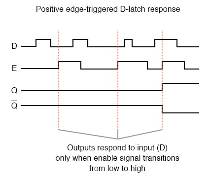
compare timing diagrams for a normal D latch versus one that is edge-triggered:

Regular D latch response
Positive edge triggered D latch response

Implementing this timing function with semiconductor components is actually quite easy, as it exploits the inherent time delay within every logic gate (known as propagation delay). What we do is take an input signal and split it up two ways, then place a gate or a series of gates in one of those signal paths just to delay it a bit, then have both the original signal and its delayed counterpart enter into a two-input gate that outputs a high signal for the brief moment of time that the delayed signal has not yet caught up to the low-to-high change in the non-delayed signal. An example circuit for producing a clock pulse on a low-to-high input signal transition is shown here:

Low to high input signal transition

This circuit may be converted into a negative-edge pulse detector circuit with only a change of the final gate from AND to NOR:

Negative edge pulse detector circuit

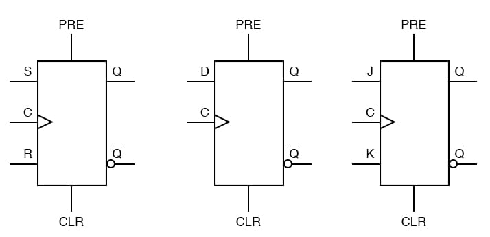
The block symbols for flip-flops are slightly different from that of their respective latch counterparts:

The triangle symbol next to the clock inputs tells us that these are edge-triggered devices, and consequently that these are flip-flops rather than latches. The symbols above are positive edge-triggered: that is, they “clock” on the rising edge (low-to-high transition) of the clock signal. Negative edge-triggered devices are symbolized with a bubble on the clock input line:

  • flip-flop is a latch circuit with a “pulse detector” circuit connected to the enable (E) input, so that it is enabled only for a brief moment on either the rising or falling edge of a clock pulse.
  • Pulse detector circuits may be made from time-delay relays for ladder logic applications, or from semiconductor gates (exploiting the phenomenon of propagation delay).

J-K Flip-Flop

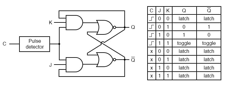
Another variation on a theme of bistable multivibrators is the J-K flip-flop. Essentially, this is a modified version of an S-R flip-flop with no “invalid” or “illegal” output state. Look closely at the following diagram to see how this is accomplished:

J K flip flop diagram
Block symbol for J-K flip flops
symbol
  • A J-K flip-flop is nothing more than an S-R flip-flop with an added layer of feedback. This feedback selectively enables one of the two set/reset inputs so that they cannot both carry an active signal to the multivibrator circuit, thus eliminating the invalid condition.
  • When both J and K inputs are activated, and the clock input is pulsed, the outputs (Q and not-Q) will swap states. That is, the circuit will toggle from a set state to a reset state or vice versa.

Asynchronous Flip-Flop Inputs

The normal data inputs to a flip flop (DS and R, or J and K) are referred to as synchronous inputs because they have an effect on the outputs (Q and not-Q) only in step, or in sync, with the clock signal transitions.

These extra inputs that I now bring to your attention are called asynchronous because they can set or reset the flip-flop regardless of the status of the clock signal. Typically, they’re called preset and clear:

Asynchronous flip flops inputs diagram three

When the preset input is activated, the flip-flop will be set (Q=1, not-Q=0) regardless of any of the synchronous inputs or the clock. When the clear input is activated, the flip-flop will be reset (Q=0, not-Q=1), regardless of any of the synchronous inputs or the clock.
So, what happens if both preset and clear inputs are activated? Surprise, surprise: we get an invalid state on the output, where Q and not-Q go to the same state, the same as our old friend, the S-R latch!

  • Asynchronous inputs on a flip-flop have control over the outputs (Q and not-Q) regardless of clock input status.
  • These inputs are called the preset (PRE) and clear (CLR). The preset input drives the flip-flop to a set state while the clear input drives it to a reset state.
  • It is possible to drive the outputs of a J-K flip-flop to an invalid condition using the asynchronous inputs, because all feedback within the multivibrator circuit is overridden.

SPI Protocol

introduction-to-spi-interface

To write code for a new SPI device you need to note a few things:

  • What is the maximum SPI speed your device can use? This is controlled by the first parameter in SPISettings. If you are using a chip rated at 15 MHz, use 15000000. Arduino will automatically use the best speed that is equal to or less than the number you use with SPISettings.
  • Is data shifted in Most Significant Bit (MSB) or Least Significant Bit (LSB) first? This is controlled by second SPISettings parameter, either MSBFIRST or LSBFIRST. Most SPI chips use MSB first data order.
  • Is the data clock idle when high or low? Are samples on the rising or falling edge of clock pulses? These modes are controlled by the third parameter in SPISettings.
SPI.beginTransaction(SPISettings(4000000,MSBFIRST,SPI_MODE0));

in arduino uno we have 16 MHZ clock speed so the maximum speed is 16000000 clocks

SPI.setClockDivider(SPI_CLOCK_DIV4)// 16/4 = 4 MHZ

calls beginTransaction a second time, the setting are maintained. You should attempt to minimize the time between before you call SPI.endTransaction(), for best compatibility if your program is used together with other libraries which use SPI.

With most SPI devices, after SPI.beginTransaction(), you will write the
slave select pin LOW, call SPI.transfer() any number of times to transfer data, then write the SS pin HIGH, and finally call SPI.endTransaction().

The extended API can use pins 4, 10, and 52 for CS.

Use

You must specify each pin you wish to use as CS for the SPI devices.

It is possible for the Due to automatically handle the chip selection between multiple devices sharing the SPI bus. Each device may have also different attribues such as speed and datamode.

If using multiple devices with different CS pins, you’ll need to declare those pins in setup(). In the following example, there are two devices that share the SPI MISO, MOSI, and SCK pins. One device CS is attached to pin 4, the other to pin 10.

void setup(){
// initialize the bus for a device on pin 4
  SPI.begin(4);
// initialize the bus for a device on pin 10
  SPI.begin(10);

Once a pin has been declared as a CS pin, it’s possible to change its default behaviors as well. For example, if the devices run at different clock speeds, the setup() may look like this :

void setup(){
// initialize the bus for the device on pin 4
  SPI.begin(4);
// Set clock divider on pin 4 to 21
  SPI.setClockDivider(4, 21);
// initialize the bus for the device on pin 10
  SPI.begin(10);
// Set clock divider on pin 10 to 84
  SPI.setClockDivider(10, 84);
}

A single byte transfer to a device on pin 4 could look like this :

void loop(){
  byte response = SPI.transfer(4, 0xFF);
}

In the above, “0xFF” is sent to the SPI device on pin 4 and the data coming from MISO is saved inside the variable response. The chip selection is handled automatically by the SPI controller, the transfer command implies the following:

  • Select device by setting pin 4 to LOW
  • Send 0xFF through the SPI bus and return the byte received
  • Deselect device by setting pin 4 to HIGH

It’s possible to send more than one byte in a transaction by telling the the transfer command to not deselect the SPI device after the transfer :

void loop(){
//transfer 0x0F to the device on pin 10, keep the chip selected
SPI.transfer(10, 0xF0, SPI_CONTINUE);
//transfer 0x00 to the device on pin 10, keep the chip selected
SPI.transfer(10, 0×00, SPI_CONTINUE);
//transfer 0x00 to the device on pin 10, store byte received in response1, keep the chip selected
byte response1 = SPI.transfer(10, 0×00, SPI_CONTINUE);
//transfer 0x00 to the device on pin 10, store byte received in response2, deselect the chip
byte response2 = SPI.transfer(10, 0×00);
}

The parameter SPI_CONTINUE ensures that chip selection is keep active between transfers. On the last transfer SPI_CONTINUE is not specified as it’s the last byte transferred.

See the individual reference pages for setClockDivider(), setDataMode(), transfer(), setBitOrder() for proper syntax when using the extended methods.

NB : once SPI.begin() is called, the declared pin will not be available as a general purpose I/O pin

//arduino uno master 
#include<SPI.h>
void setup() {
   digitalWrite(SS, HIGH); // disable Slave Select
   SPI.begin();
   SPI.setClockDivider(SPI_CLOCK_DIV4);//divide the clock by 4
}
void loop() {
   char c;
   digitalWrite(SS, LOW); // enable Slave Select
   for (const char * p = "Hello Mega\r" ; c = *p; p++) 
   {
      SPI.transfer(c);
   }
   digitalWrite(SS, HIGH); // disable Slave Select
   delay(2000);
}
//arduino mega slave
#include<SPI.h>
char buff [50];
volatile byte indx;
volatile boolean process;

void setup (void) {
   Serial.begin (9600);
   pinMode(MISO, OUTPUT); // have to send on master in so it set as output
   SPCR |= _BV(SPE); // turn on SPI in slave mode
   indx = 0; // buffer empty
   process = false;
   SPI.attachInterrupt(); // turn on interrupt
}

ISR (SPI_STC_vect) // SPI interrupt routine 
{ 
   byte c = SPDR; // read byte from SPI Data Register
   if (indx < sizeof buff) {
      buff [indx++] = c; // save data in the next index in the array buff
      if (c == '\r') //check for the end of the word
      process = true;
   }
}

void loop (void) {
   if (process) {
      process = false; //reset the process
      Serial.println (buff); //print the array on serial monitor
      indx= 0; //reset button to zero
   }
}
//master esp32 arduino
#include <Arduino.h>
#include <SPI.h>
SPIClass spi;
void setup() {
  Serial.begin(9600);
  spi=SPIClass(VSPI);
  spi.begin();
  pinMode(5,OUTPUT);
  digitalWrite(5,HIGH);
}

void loop() { 
  delay(5000);
  digitalWrite(5,LOW);
  spi.beginTransaction(SPISettings(4000000,MSBFIRST,SPI_MODE0));
  spi.transfer(99);
  digitalWrite(5,HIGH);
  spi.endTransaction();
}
use spi with 74ch165

I2C Protocol

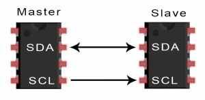
I2C combines the best features of SPI and UARTs. With I2C, you can connect multiple slaves to a single master (like SPI) and you can have multiple masters controlling single, or multiple slaves. This is really useful when you want to have more than one microcontroller logging data to a single memory card or displaying text to a single LCD.

Like UART communication, I2C only uses two wires to transmit data between devices:

Introduction to I2C - Single Master Single Slave

SDA (Serial Data) – The line for the master and slave to send and receive data.

SCL (Serial Clock) – The line that carries the clock signal.

Note: in many breakout boards, the SDA line may also be labeled as SDI and the SCL line as SCK.

I2C is a serial communication protocol, so data is transferred bit by bit along a single wire (the SDA line).

Like SPI, I2C is synchronous, so the output of bits is synchronized to the sampling of bits by a clock signal shared between the master and the slave. The clock signal is always controlled by the master.

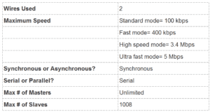
Basics of the I2C Communication Protocol - Specifications Table

HOW I2C WORKS

With I2C, data is transferred in messages. Messages are broken up into frames of data. Each message has an address frame that contains the binary address of the slave, and one or more data frames that contain the data being transmitted. The message also includes start and stop conditions, read/write bits, and ACK/NACK bits between each data frame:

Introduction to I2C - Message, Frame, and Bit

Start Condition: The SDA line switches from a high voltage level to a low voltage level before the SCL line switches from high to low.

Stop Condition: The SDA line switches from a low voltage level to a high voltage level after the SCL line switches from low to high.

Address Frame: A 7 or 10 bit sequence unique to each slave that identifies the slave when the master wants to talk to it.

Read/Write Bit: A single bit specifying whether the master is sending data to the slave (low voltage level) or requesting data from it (high voltage level).

ACK/NACK Bit: Each frame in a message is followed by an acknowledge/no-acknowledge bit. If an address frame or data frame was successfully received, an ACK bit is returned to the sender from the receiving device.

ADDRESSING

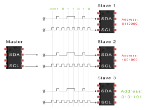
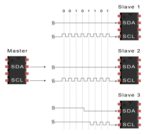
I2C doesn’t have slave select lines like SPI, so it needs another way to let the slave know that data is being sent to it, and not another slave. It does this by addressing. The address frame is always the first frame after the start bit in a new message.

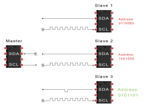
The master sends the address of the slave it wants to communicate with to every slave connected to it. Each slave then compares the address sent from the master to its own address. If the address matches, it sends a low voltage ACK bit back to the master. If the address doesn’t match, the slave does nothing and the SDA line remains high.

READ/WRITE BIT

The address frame includes a single bit at the end that informs the slave whether the master wants to write data to it or receive data from it. If the master wants to send data to the slave, the read/write bit is a low voltage level. If the master is requesting data from the slave, the bit is a high voltage level.

THE DATA FRAME

After the master detects the ACK bit from the slave, the first data frame is ready to be sent.

The data frame is always 8 bits long, and sent with the most significant bit first. Each data frame is immediately followed by an ACK/NACK bit to verify that the frame has been received successfully. The ACK bit must be received by either the master or the slave (depending on who is sending the data) before the next data frame can be sent.

After all of the data frames have been sent, the master can send a stop condition to the slave to halt the transmission. The stop condition is a voltage transition from low to high on the SDA line after a low to high transition on the SCL line, with the SCL line remaining high.

STEPS OF I2C DATA TRANSMISSION

1. The master sends the start condition to every connected slave by switching the SDA line from a high voltage level to a low voltage level before switching the SCL line from high to low:

Introduction to I2C - Data Transmission Diagram START CONDITION

2. The master sends each slave the 7 or 10 bit address of the slave it wants to communicate with, along with the read/write bit:

Introduction to I2C - Data Transmission Diagram ADDRESS FRAME

3. Each slave compares the address sent from the master to its own address. If the address matches, the slave returns an ACK bit by pulling the SDA line low for one bit. If the address from the master does not match the slave’s own address, the slave leaves the SDA line high.

Introduction to I2C - Data Transmission Diagram ACK Bit Slave to Master

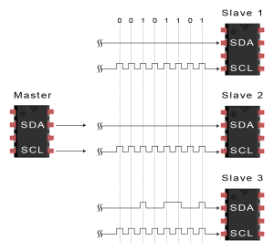
4. The master sends or receives the data frame:

Introduction to I2C - Data Transmission Diagram Data Frame

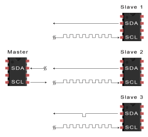
5. After each data frame has been transferred, the receiving device returns another ACK bit to the sender to acknowledge successful receipt of the frame:

Introduction to I2C - Data Transmission Diagram ACK Bit Slave to Master

6. To stop the data transmission, the master sends a stop condition to the slave by switching SCL high before switching SDA high:

Introduction to I2C - Data Transmission Diagram Stop Condition

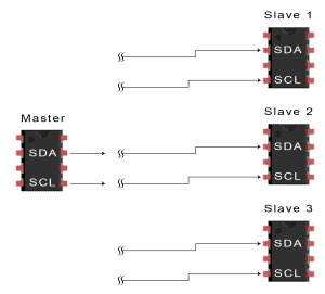
SINGLE MASTER WITH MULTIPLE SLAVES

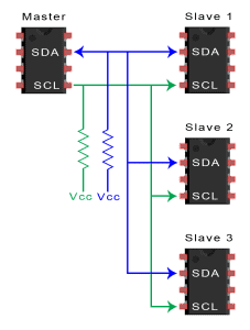
Because I2C uses addressing, multiple slaves can be controlled from a single master. With a 7 bit address, 128 (27) unique address are available. Using 10 bit addresses is uncommon, but provides 1,024 (210) unique addresses. To connect multiple slaves to a single master, wire them like this, with 4.7K Ohm pull-up resistors connecting the SDA and SCL lines to Vcc:

Introduction to I2C - Single Master Multiple Slaves

MULTIPLE MASTERS WITH MULTIPLE SLAVES

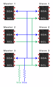
Multiple masters can be connected to a single slave or multiple slaves. The problem with multiple masters in the same system comes when two masters try to send or receive data at the same time over the SDA line. To solve this problem, each master needs to detect if the SDA line is low or high before transmitting a message. If the SDA line is low, this means that another master has control of the bus, and the master should wait to send the message. If the SDA line is high, then it’s safe to transmit the message. To connect multiple masters to multiple slaves, use the following diagram, with 4.7K Ohm pull-up resistors connecting the SDA and SCL lines to Vcc:

Introduction to I2C - Multiple Masters Multiple Slaves 2

ADVANTAGES AND DISADVANTAGES OF I2C

There is a lot to I2C that might make it sound complicated compared to other protocols, but there are some good reasons why you may or may not want to use I2C to connect to a particular device:

ADVANTAGES

  • Only uses two wires
  • Supports multiple masters and multiple slaves
  • ACK/NACK bit gives confirmation that each frame is transferred successfully
  • Hardware is less complicated than with UARTs
  • Well known and widely used protocol

DISADVANTAGES

  • Slower data transfer rate than SPI
  • The size of the data frame is limited to 8 bits
  • More complicated hardware needed to implement than SPI